描述
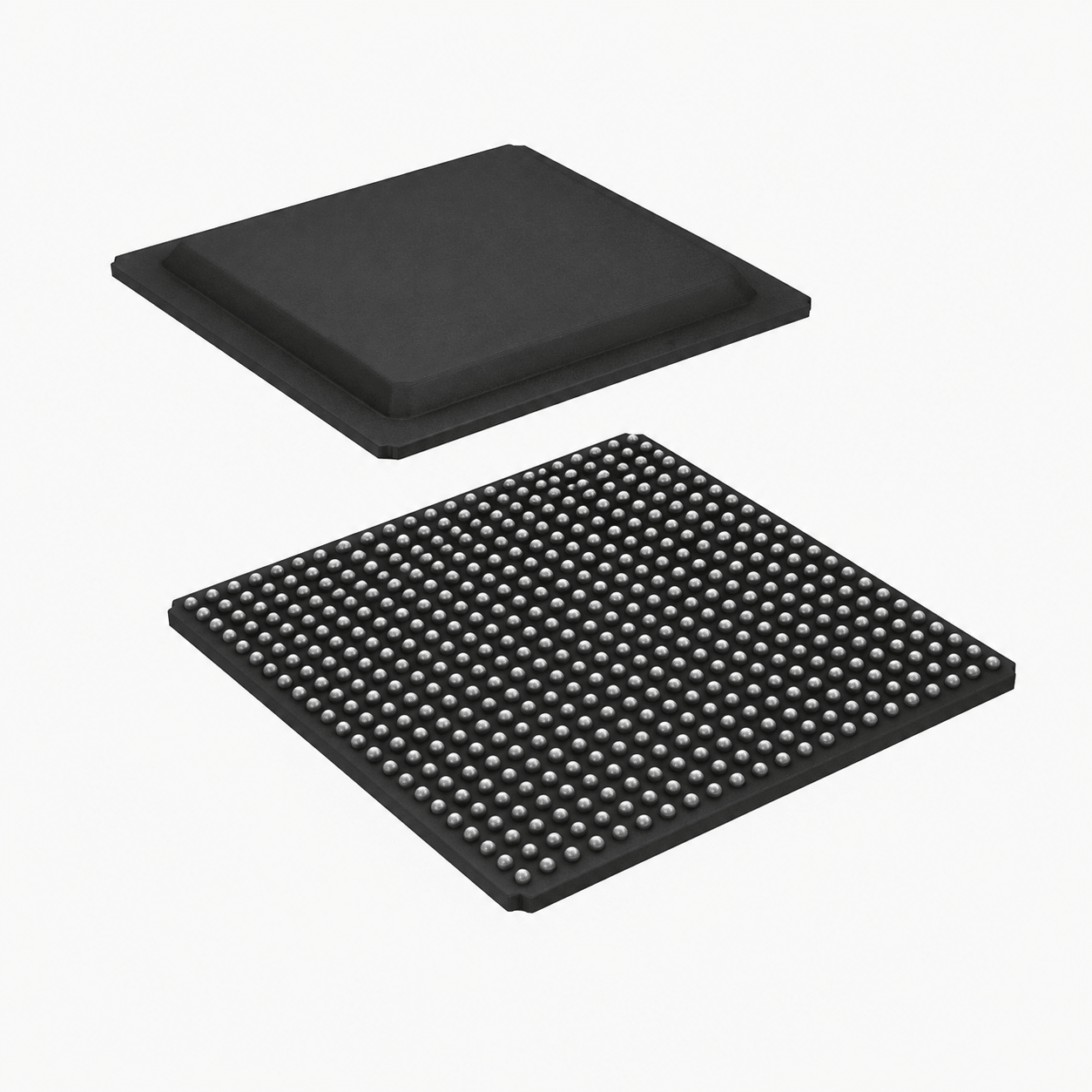
XC7A100T-2FGG484C Artix-7 FPGA
Flagship Logic Density meets Power Optimization – The Professional Artix-7 100T FPGA Choice for Advanced Signal Bridging & Massive Parallel Computing.
// High-Capacity 101.4K Logic Cells Programmable Fabric Portfolio
The Artix-7 100T Performance Edge
The XC7A100T-2FGG484C stands as the ultimate density choice for power-conscious, budget-optimized embedded designs requiring intensive data processing throughput. Engineered by AMD Xilinx on a cutting-edge 28-nm high-k metal gate (HKMG) process, this Artix-7 FPGA steps up system integration by packing 101,440 high-performance logic cells and an expansive 4,860 Kbits internal block RAM pool. Housed in a low-inductive FBGA484 package footprint, it delivers immense parallel algorithmic execution across 285 user-configurable I/O ports, successfully wiping out bus bottlenecks in multi-channel video grids and telecommunication mainboards.
- 101,440 High-efficiency Logic Cells for massive hardware logic pooling
- 285 Configurable User I/O pins optimized for high-speed voltage rail drive
- Integrated digital signal processing (DSP) slices and global PLL networks
Key Performance Advantages
101K LEs High Capacity
Provides 101,440 logical cells, easily accommodating extensive intellectual property (IP) cores, soft processors, and custom algorithmic logic blocks inside one chip.
4,860Kb Block RAM
Houses a large internal block RAM matrix, allowing smooth deep dual-port FIFO streams, real-time data caching, and dense video/telemetry packet buffering routines.
Massive 285 User I/O
Expands external interface capabilities with 285 programmable pins, backed by multi-frequency clock managers to stabilize wide bus interactions under intense EMI.
Technical Specifications
| Parameter Node | Detailed Engineering Specification |
|---|---|
| Manufacturer | AMD Xilinx |
| Part Number (MPN) | XC7A100T-2FGG484C |
| Device Family | Artix-7 FPGA Architecture Series |
| Logic Cells / Elements | 101,440 Logic Cells |
| Total Embedded RAM | 4,860 Kbits (4.86 Mb Internal Block RAM Matrix) |
| Number of LABs / CLBs | 7,925 Logic Array Blocks |
| Number of User I/Os | 285 Configurable User I/O Ports |
| Package / Case Form | FBGA-484 / FGG484 Footprint (Fine-Pitch Ball Grid Array Package, 23mm x 23mm) |
| Speed Grade Designation | -2 Speed Optimization Grade |
| Temperature Window | 0°C to +85°C Commercial Operational Spectrum Compliance |
Versatile Hardware Applications
- Advanced Image Processing: Manages real-time multi-channel medical equipment image streams and factory sorting cameras.
- Industrial Automation Controllers: Runs complex parallel algorithmic closed-loop maps inside high-axis CNC and master PLC controllers.
- High-Speed Interface Bridging: Ideal for multi-gigabit custom PCIe extensions, network switches, and protocol level-shifting.
- System Logic Consolidation: Cleanly integrates massive discrete processors and logic arrays onto one single secure chip canvas.
Industrial Quality Protections
100% Original Sourcing: Procured securely through fully audited tier-1 franchise lines, completely ensuring anti-counterfeit protection.
Anti-Static Handling: Stored and picked in full alignment with international ANSI/ESD cleanroom facility benchmarks.
Full Batch Traceability: Verified via intensive certificate analysis and rigorous documentation tracking prior to export dispatch.
HIGH-PERFORMANCE PROGRAMMABLE LOGIC SOLUTIONS // DIRECT SOURCE ARCHITECTURE