描述
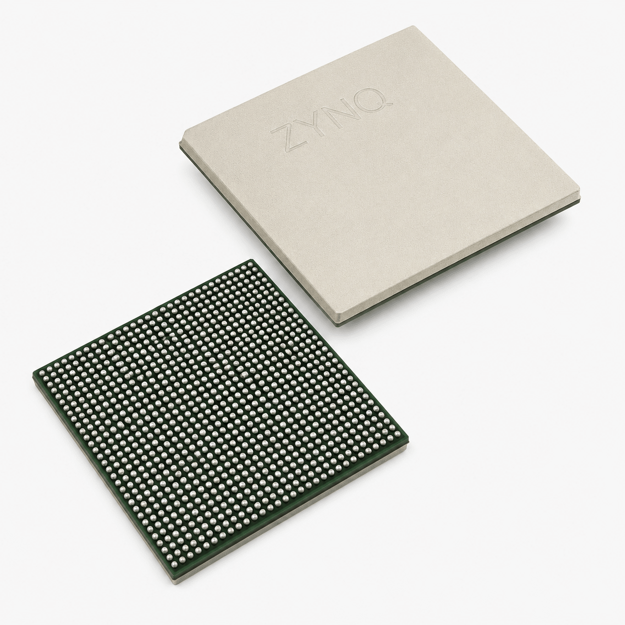
XC7K325T-2FFG900C Kintex-7 FPGA
High-Bandwidth Performance meets Advanced DSP Power – The Professional Kintex-7 Mainstream FPGA Choice for Signal Processing & Multi-Gigabit Transceivers.
// High-Density 326K Logic Cells Programmable Fabric Portfolio
The Kintex-7 High-Density Advantage
The XC7K325T-2FFG900C represents a premium industry standard for cost-efficient, high-bandwidth programmable logic design. Engineered by AMD Xilinx on an advanced 28-nm state-of-the-art architecture, this Kintex-7 FPGA integrates a substantial 326,080 flexible logic cells alongside a massive 16,020 Kbits block RAM matrix. Housed in a dense, multi-ball FBGA900 package footprint, it delivers exceptional parallel processing throughput across 500 user-configurable I/O ports, successfully preventing critical transmission bottlenecks inside telecommunication infrastructure and medical visualization subsystems.
- 326,080 high-efficiency Logic Cells for dense custom hardware gating partitions
- 500 Configurable User I/O pins optimized for multi-voltage interface rail drive
- Integrated multi-frequency global clock networks and high-performance DSP slices
Key Performance Advantages
Advanced 28nm Fabric
Built on a power-optimized 28-nm architectural process node, minimizing static power consumption while maintaining superior logic cell compute frequencies.
16,020Kb Block RAM
Houses a massive internal memory block matrix, providing smooth ultra-deep dual-port buffering pipelines and large data packet caching without stalls.
Massive 500 User I/O
Expands hardware connectivity with 500 programmable user pins, backed by integrated GTX transceivers to secure deterministic signal tracking paths.
Technical Specifications
| Parameter Node | Detailed Engineering Specification |
|---|---|
| Manufacturer | AMD Xilinx |
| Part Number (MPN) | XC7K325T-2FFG900C |
| Device Family | Kintex-7 FPGA Architecture Series |
| Logic Cells / Elements | 326,080 Logic Cells |
| Total Embedded RAM | 16,020 Kbits (16.02 Mb Internal Block RAM Matrix) |
| Number of LABs / CLBs | 25,475 Logic Array Blocks |
| Number of User I/Os | 500 Configurable User I/O Ports |
| Package / Case Form | FCBGA-900 / FFG900 Footprint (Flip-Chip Ball Grid Array, 31mm x 31mm body) |
| Speed Grade Designation | -2 Speed Optimization Grade |
| Temperature Window | 0°C to +85°C Commercial Operational Spectrum Compliance |
Versatile Hardware Applications
- Telecommunications Infrastructure: Central data routers, high-frequency base stations, and optical transport framing lines.
- High-Speed Signal Processing: Perfect for complex algorithmic math matrices, software-defined radio (SDR), and radar arrays.
- Advanced Video Routing: High-bandwidth 4K/8K video processing, image filtering matrix channels, and multi-display hubs.
- PCI Express Interfacing: Ideal for complex hardware acceleration slots, data streaming servers, and custom system endpoints.
Industrial Quality Protections
100% Original Sourcing: Procured securely through fully audited tier-1 franchise lines, completely ensuring anti-counterfeit protection.
Anti-Static Handling: Stored and picked in full alignment with international ANSI/ESD cleanroom facility benchmarks.
Full Batch Traceability: Verified via intensive certificate analysis and rigorous documentation tracking prior to export dispatch.
HIGH-PERFORMANCE PROGRAMMABLE LOGIC SOLUTIONS // DIRECT SOURCE ARCHITECTURE