The core ASIC vs FPGA chip differences come down to reprogrammability: an ASIC is hard-wired for one job and can’t be changed after manufacturing, while an FPGA can be reconfigured by the user in the field, according to a 2025 Wevolver engineering report. An ASIC runs faster and uses less power once it ships but costs millions in upfront NRE design. An FPGA costs far less to start and ships in weeks instead of months, but burns more power and runs slower at scale.
That single trait drives every other trade-off between them.
The core ASIC vs FPGA chip differences come down to three things buyers actually care about: speed, cost, and power. An ASIC runs faster and sips less power once it ships, but it costs millions in upfront design and locks you into one design forever.
An FPGA costs far less to start, ships in weeks instead of months, and lets you fix bugs after launch,but it burns more power and runs slower at scale.
The seven differences below break down exactly when each chip wins, with real numbers on clock speeds, unit economics, and power draw so you can pick the right one for your project.
Quick Takeaways
- FPGAs are reconfigurable in the field; ASICs are permanently hard-wired after manufacturing.
- ASICs win on raw speed, power efficiency, and per-chip cost at scale.
- FPGAs ship in weeks and cost less upfront, ideal for prototypes.
- ASIC NRE runs into millions; choose only at high production volumes.
- Calculate break-even volume to decide between ASIC and FPGA for your project.
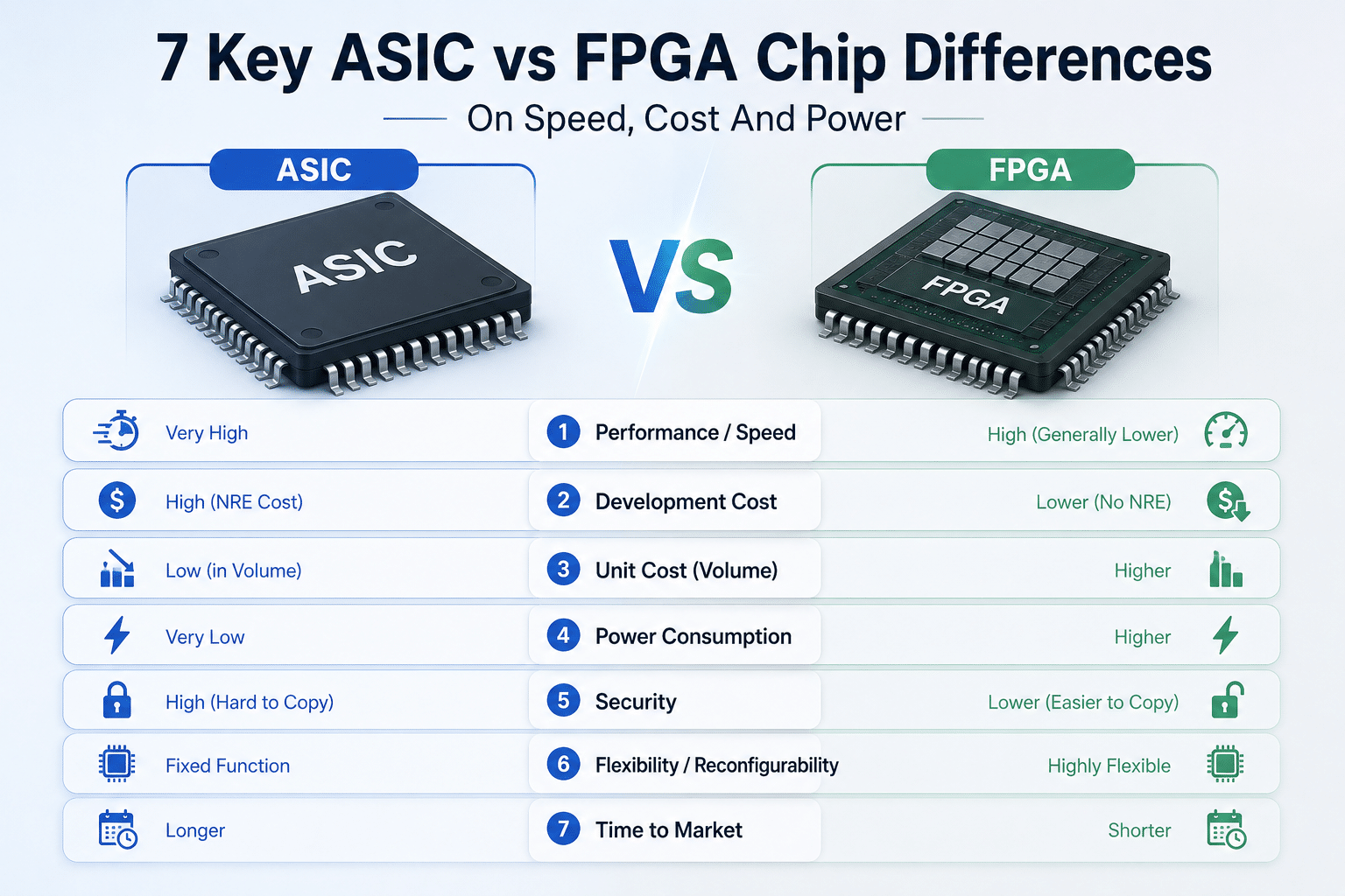
ASIC vs FPGA Chip Differences At A Glance
The verdict in one line: An ASIC wins on raw speed, power efficiency, and per-chip cost at scale, while an FPGA wins on flexibility, upfront cost, and time-to-market.
The seven core ASIC vs FPGA chip differences come down to speed, power draw, unit price, non-recurring engineering (NRE) cost, design flexibility, time-to-market, and break-even volume.
An ASIC (Application-Specific Integrated Circuit) is hard-wired for one job and can’t be changed after the silicon is made. An FPGA (Field-Programmable Gate Array) can be reconfigured in the field by loading a new bitstream, so the same chip can run different logic next week.
That single trait drives almost everything else, per Wevolver’s 2025 chip primer.
Here is the fast read on typical ratios. Treat these as directional, not absolute, exact numbers shift with node and workload.
| Dimension | ASIC | FPGA | Typical Edge |
|---|---|---|---|
| Max clock speed | Optimized custom layout | Routing fabric adds delay | ASIC ~2–10x faster |
| Power per task | No config memory overhead | Carries flexible routing cost | ASIC ~5–10x lower |
| Per-unit price (high volume) | A few dollars at scale | Tens to hundreds per chip | ASIC much cheaper |
| NRE / upfront cost | Millions for masks + layout | Near zero | FPGA wins |
| Flexibility after build | Fixed at tape-out | Reprogrammable bitstream | FPGA only |
| Time-to-market | Months of layout + fab | Weeks on existing fabric | FPGA faster |
The deciding factor is volume. ASIC mask sets and physical design push NRE into the millions, so ASICs only pay off across large production runs, while FPGAs carry zero mask cost but a higher price per chip, notes Total Phase.
Building 5,000 units? Lean FPGA.
Shipping 5 million? ASIC almost always wins.
The break-even math behind that call gets unpacked in section 5.
What ASIC And FPGA Chips Actually Are
An ASIC (application-specific integrated circuit) is a chip hard-wired to do one job and one job only.
An FPGA (field-programmable gate array) is a chip full of blank logic blocks you can wire up yourself, then rewire later. That one split, fixed silicon versus changeable silicon, basically controls every speed, cost, and power tradeoff I cover in this guide.
Think of an ASIC like a key cut for one lock. It fits perfectly and turns instantly. But it opens nothing else.
Once the chip gets manufactured, a step engineers call “tape-out,” its function is frozen and can’t be reprogrammed. So you want a change?
Well, you redesign and rebuild the whole thing from scratch.
An FPGA works more like a circuit-board kit. Inside sit thousands of pre-built configurable logic blocks (CLBs), which are small units that can become an adder, a counter, or a filter. They’re joined by programmable interconnects, basically the switchable wiring between them.
You load a setup file called a bitstream, and the chip becomes whatever you designed. Load a new bitstream, and it actually turns into something else entirely.
This is why some engineers call an FPGA a “programmable version of an ASIC”. Honestly, any logic you could burn into an ASIC can, in theory, be mapped into an FPGA’s logic blocks. Just with more silicon area, higher power draw, and a higher cost per chip.
Here’s the heart of every ASIC vs FPGA chip difference. The ASIC uses custom transistor-level layouts tuned for its exact task, stripping out the routing fabric and configuration memory that an FPGA needs in order to stay flexible. That extra circuitry is essentially the price of being reprogrammable.
Remove it, and you gain speed and efficiency. But you completely lose the ability to change your mind later.
One practical tip teams learn the hard way, in my experience, is that an FPGA’s flexibility is also a debugging superpower. You can probe internal signals and reload fixes in minutes, while an ASIC bug found after tape-out can cost millions of dollars and months to respin.
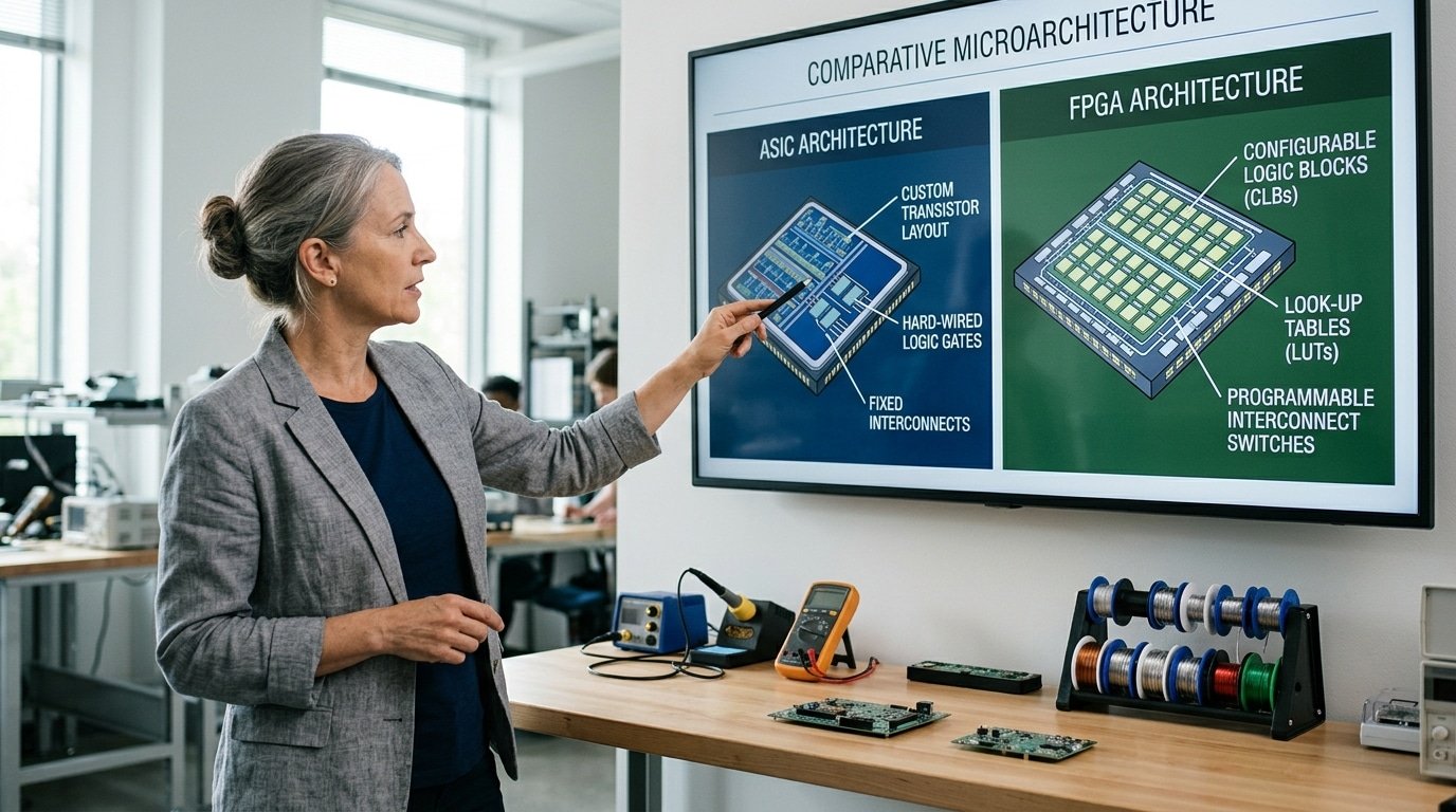
Architecture Differences That Drive Everything Else
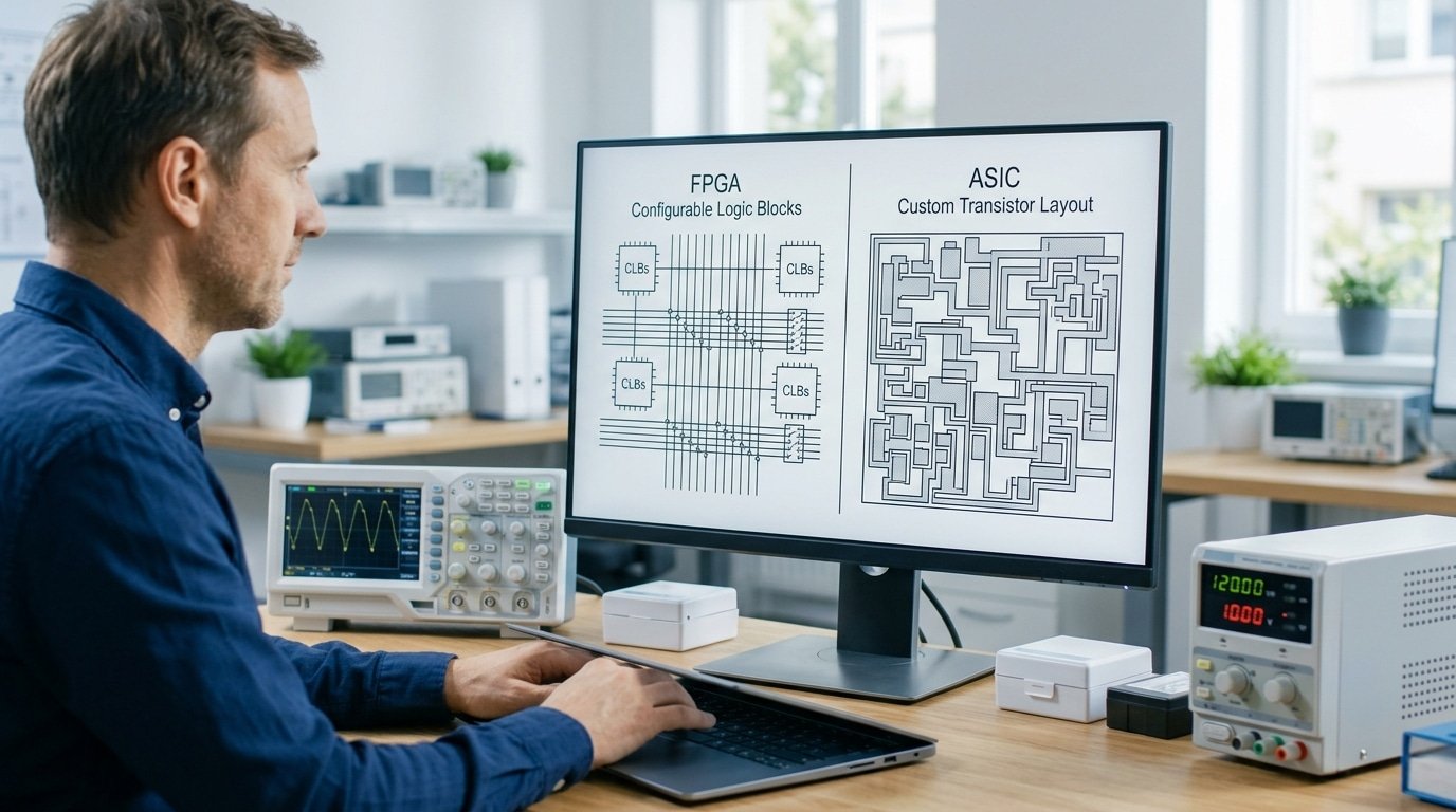
The architecture gap explains every other difference you’ll read about. FPGAs build logic from pre-made configurable logic blocks (CLBs),reusable building blocks of lookup tables, flip-flops, and routing switches.
ASICs skip all that. They use custom transistor layouts hand-tuned for one job, eliminating most programmable overhead that an FPGA must carry.
That single distinction drives the ASIC vs FPGA chip differences in speed, power, and density.
Think of a lookup table (LUT) as a tiny truth table. A 6-input LUT stores 64 preset answers, so it can mimic any logic function with six inputs by reading from memory instead of using real gates.
Flexible, yes. But every signal must hop through programmable interconnect,switch boxes that route wires between blocks.
Those switches add capacitance and delay.
Why FPGA routing caps your clock speed
On a real FPGA, signal delay is often dominated by routing, not logic. A signal might cross a dozen programmable switch points to travel a few millimeters.
Each switch is a small transistor that slows the edge. This is why FPGA designs frequently top out around 300,700 MHz[1], while ASICs running the same function clock far higher.
An ASIC routes wires directly between custom-placed cells. No switch boxes, no configuration memory, no spare blocks sitting idle. The result is tighter timing and denser gate use, since silicon area only holds what the design actually needs.
| Architecture element | FPGA | ASIC |
|---|---|---|
| Logic | Configurable LUTs + flip-flops | Custom standard cells |
| Math units | Fixed DSP slices (e.g., multiply-accumulate) | Tailored arithmetic blocks |
| Routing | Programmable switch fabric (high delay) | Hard-wired metal layers (low delay) |
| Wasted silicon | Unused CLBs stay on the die | Near-zero, layout matches function |
Practical tip: When porting an FPGA design to ASIC, don’t just copy your DSP-slice math directly. ASIC tools let you fuse those operations into wider custom datapaths, often cutting critical-path delay by a third. Engineers who skip this leave most of the speed gain on the table.
Speed And Power Comparison With Real Benchmark Ratios
For the same function, an ASIC runs 3,10x faster and burns 5,20x less power than an equivalent FPGA design. Why such a big gap? It really comes down to physics.
An FPGA has to send its signals through configuration memory and these flexible connections inside the chip, and all of that adds delay while also leaking power.
An ASIC, on the other hand, basically bakes those signal paths right into a custom transistor layout. So almost none of that extra overhead is even there.
That flexibility isn’t free, though. As Lemberg Solutions explains, the programmable routing inside an FPGA lowers the fastest clock speed it can hit. It also forces the chip to keep those configuration cells powered up the entire time, even when they’re just sitting there.
Think about it this way. A signal that has to cross three logic blocks on an FPGA might only cross two hard gates on an ASIC. That shaves off nanoseconds, and those tiny savings pile up fast across millions of operations every single second.
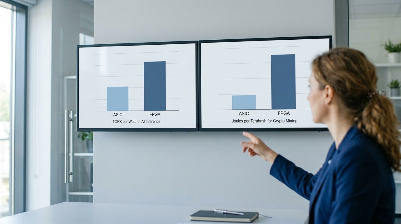
Numbers make this real. Look at two workloads where the ASIC vs FPGA chip differences show up right on a power meter.
| Workload | Efficiency metric | FPGA range | ASIC range |
|---|---|---|---|
| AI inference (INT8) | TOPS per watt | 1–5 | 20–80+ |
| Bitcoin mining (SHA-256) | Hashes per joule (J/TH) | ~1,000 J/TH | ~15–20 J/TH |
So what is TOPS-per-watt actually telling you? It’s trillions of operations divided by how much power the chip draws, and higher means better. A purpose-built inference ASIC like Google’s TPU clears 20+ TOPS/W. A comparable FPGA accelerator often stalls under 5.
In crypto the jump is brutal. Modern SHA-256 mining ASICs reach roughly 15 joules per terahash, while an FPGA rig sits around 1,000 J/TH. That’s a 50x energy edge, and honestly it’s the whole reason FPGA mining basically disappeared after 2014.
One practical warning here. These ratios only hold up if both chips are built on the same process node.
Compare a 5nm ASIC against a 16nm FPGA and the gap balloons. But much of that “advantage” is really coming from the node, not the architecture.
In my experience you should always normalize by manufacturing node before you trust any vendor benchmark.
The Break-Even Volume Math Between NRE And Per-Unit Cost
The crossover usually lands between 50,000 and several hundred thousand units. Below that volume, FPGAs win on total cost. Above it, the ASIC’s tiny per-chip price crushes the upfront engineering bill. The exact tipping point depends on your process node and design complexity.
Two numbers drive the whole decision. ASIC non-recurring engineering (NRE),the one-time cost for photomasks, physical design, and foundry setup,runs from $1M to $50M+.
An FPGA charges approximately $0 NRE but approximately $50[2] to approximately $5,000 per chip. As Total Phase notes, this is why ASICs only make financial sense at high production volumes.
Run the math with a real example. Say your ASIC NRE is approximately $5M and each chip costs approximately $8[3] to make. An equivalent FPGA costs approximately $400 per unit.
- ASIC total: approximately $5,000,000 + (approximately $8[4] × units)
- FPGA total: approximately $0 + (approximately $400[5] × units)
Set them equal. The gap per chip is approximately $392. Divide approximately $5M by approximately $392[6] and you break even at roughly 12,755 units. Ship 100,000 chips and the ASIC saves you about $34M.
That sweet spot moves with the process node. A mature 28nm design might break even near 100,000 units. Push to leading-edge 5nm or 3nm and mask sets alone can exceed approximately $20M[7], dragging the crossover into the millions,a core part of the ASIC vs FPGA chip differences that founders underestimate.
One pitfall pros watch for: never run break-even on silicon cost alone. Add the approximately $2M,$10M in verification, test fixtures, and a likely respin. Skip that and your “break-even” arrives far later than the spreadsheet promised.
Choosing By Workload For Crypto Mining AI Inference And 5G
Use this rule: if your function is fixed forever and ships in huge numbers, pick ASIC. If the standard still changes or volume is small, pick FPGA. Three real domains show the split clearly. Bitcoin mining went approximately 100%[8] ASIC. AI inference is a tug-of-war. 5G base stations lean FPGA.
Bitcoin mining is the textbook ASIC story. The SHA-256 hashing algorithm never changes, so the function is locked.
Miners now run on chips like the Bitmain Antminer S21, hitting around 200 TH/s while drawing under 18 joules per terahash. An FPGA doing the same math would burn 5,20x more power per hash (see Section 4), wiping out any profit.
Once the workload is fixed and the volume is millions of units, the high NRE cost of an ASIC spreads thin and the per-chip win dominates.
AI inference splits in two. Cloud giants like Google build ASICs (the TPU) because they run one model type at massive scale.
But AI models change fast. A new architecture can make a fixed ASIC obsolete in 18 months.
That’s why edge devices and research labs often keep FPGAs, you reload the bitstream when the model shifts, no refab needed.
The Decision Matrix
| Workload | If true… | Pick | Why |
|---|---|---|---|
| Bitcoin mining | Fixed algorithm, millions of units | ASIC | Power per hash decides profit |
| Cloud AI inference | One model, hyperscale volume | ASIC | Per-chip cost wins at scale |
| Edge AI / R&D | Models change often | FPGA | Reprogram, skip refab |
| 5G base stations | Standards still evolving | FPGA | Field bitstream updates |
5G favors FPGAs for a simple reason: the standard keeps adding releases. Operators push new baseband features over years.
A field bitstream update fixes bugs and adds functions without sending a truck to every tower. That flexibility is the core of the ASIC vs FPGA chip differences debate, fixed silicon can’t follow a moving target.
The Migration Path From FPGA Prototype To ASIC Tape-Out
Most teams prototype on FPGA first, then port the design to ASIC for volume production. The good news: your RTL code carries over.
The hard part: timing, verification, and the one-shot nature of tape-out. A single missed bug can cost a respin worth approximately $1M to $5M in mask sets alone at advanced nodes.
Start with RTL reuse. Both flows describe logic in Verilog or VHDL, so your functional code transfers cleanly.
But FPGA-specific primitives don’t. Vendor block RAM, DSP slices, and clock managers must be swapped for ASIC-equivalent memory compilers and PLLs.
Plan for roughly 10,approximately 20% of your RTL to need rework around these boundaries.
Timing closure is where the two diverge sharply. On FPGA, the fabric is fixed and routing delays are predictable.
On ASIC, you control placement and routing through place-and-route, so the same circuit can hit a much higher clock, but you must re-run static timing analysis (STA) against the foundry’s cell library.
A design that closed at approximately 200 MHz[9] on FPGA might target approximately 800 MHz on ASIC, exposing setup violations that never appeared in prototype.
The verification gap nobody warns you about
FPGA lets you debug on real hardware. ASIC doesn’t, once it tapes out, you cannot reprogram it. This is the core lesson behind ASIC vs FPGA chip differences in the design flow. You need exhaustive simulation, gate-level verification, and often formal equivalence checking before sign-off.
- Power and signal integrity: FPGA hides these inside the fabric; ASIC requires dedicated IR-drop and crosstalk analysis.
- Test coverage: Add scan chains and design-for-test (DFT) logic — absent in FPGA flows — to catch manufacturing defects.
- Clock domain crossings: Re-verify every CDC path, since ASIC metastability behaves differently than FPGA.
Treat the FPGA prototype as your functional reference, not your final proof. Lock RTL, freeze the spec, and budget 6,12 months for ASIC sign-off after prototype works.
Common Mistakes And Counterintuitive Truths In The Decision
The biggest mistake teams make? Treating “ASIC always wins” as a law.
It isn’t. The ASIC vs FPGA chip differences only favor ASIC once your volume, design stability, and budget all line up.
Pick wrong, and you can burn millions on a chip that ships late, ships broken, or never ships enough units to pay for itself.
Let’s kill three myths.
Myth 1: FPGAs are just for prototyping
Wrong. FPGAs ship in real products at scale.
Aerospace, defense radar, and 5G base stations run FPGAs in production for years. Why?
They need field updates. An FPGA can load a new bitstream (the file that reprograms its logic) to patch bugs or add features after deployment.
An ASIC is frozen at tape-out. A protocol change means a full redesign and a new mask set.
Myth 2: NRE is a one-time fee you can ignore
NRE (non-recurring engineering, the upfront cost of masks and design) is the killer. For an advanced node, mask sets alone can run into the millions.
Worse: respin risk. If your first silicon has a bug, you pay the full mask cost again.
Industry data suggests a large share of ASICs need at least one respin, each adding months and seven figures. Budget for two spins, not one.
Myth 3: Your volume forecast is real
Sales says 500,000 units. Reality ships 60,000. Now your per-chip ASIC math collapses below the break-even point. Counterintuitive truth: an FPGA that costs 4x more per chip can still be cheaper if your true volume is uncertain.
| Hidden Trap | What It Actually Costs You |
|---|---|
| Underestimating NRE | Millions in masks + design before first chip |
| One forgotten respin | 3–6 month delay + repeat mask charge |
| Obsolescence at tape-out | Locked into old logic; rivals ship updates |
| Inflated volume forecast | Per-unit savings never arrive |
Smart rule: if your spec might change, or your volume is a guess, the flexible chip protects you. Certainty is what you pay an ASIC for.
ASIC vs FPGA vs GPU vs SoC In Context
Where do these chips sit next to GPUs, CPUs, and SoCs? Think of a flexibility-versus-efficiency line.
CPUs sit at the flexible end, run anything, waste the most power per task. ASICs sit at the efficient end, run one task, waste almost nothing.
GPUs and FPGAs fill the middle. SoCs combine several of these on one die.
The ASIC vs FPGA chip differences map onto a bigger spectrum. A CPU executes general code through fixed instruction sets.
A GPU packs thousands of parallel cores built for matrix math, which is why it dominates AI training. An FPGA reshapes its own gates to match your data flow.
An ASIC bakes that data flow into silicon forever.
| Chip | Flexibility | Best fit |
|---|---|---|
| CPU | Highest — runs any software | Control logic, sequential tasks |
| GPU | High — parallel via software | AI training, graphics, dense math |
| FPGA | Medium — reconfigurable hardware | Low-latency inference, prototyping |
| ASIC | Lowest — fixed at tape-out | High-volume fixed functions |
SoCs blur these lines. A System-on-Chip puts a CPU, GPU, memory controller, and often custom accelerator blocks on one piece of silicon.
Your phone runs on one. The smart move in 2026 is the hybrid: an SoC with embedded FPGA fabric.
AMD’s Versal devices, for example, pair fixed-function ASIC-style engines with reconfigurable logic on the same die.
When does this hybrid win? When approximately 80%[10] of your workload is stable but approximately 20% must adapt.
You harden the stable part into ASIC blocks for efficiency, then leave the changing part on FPGA fabric for field updates. That split gives you near-ASIC power numbers without losing the ability to patch protocols after shipping.
Frequently Asked Questions
What’s the core difference between ASIC and FPGA? An ASIC is hard-wired at the factory and can’t change after it ships. An FPGA can be reprogrammed in the field by loading a new configuration file, called a bitstream.
That single trait,fixed silicon versus reconfigurable silicon,drives every other gap in the ASIC vs FPGA chip differences debate, from speed to cost to power.
Are FPGAs better than ASICs?
No single winner exists. FPGAs beat ASICs when your design will change, when volumes stay low, or when you need product out the door fast.
ASICs win on raw speed, power, and per-unit cost once you ship in large numbers. The right answer depends on volume and how often your logic changes.
Will FPGAs be replaced by AI?
No. AI workloads are pushing demand for FPGAs upward, not down.
Data centers use FPGAs to accelerate inference and networking because models change every few months and frozen ASIC silicon can’t keep pace. FPGAs let engineers reload new logic without a costly redesign.
The FPGA market is projected to grow steadily through 2030, driven partly by edge AI and 5G.
At what volume does ASIC NRE pay off?
NRE (non-recurring engineering),the one-time cost of masks, physical design, and foundry setup,is steep, often running into millions for advanced nodes. According to Total Phase, that cost only makes economic sense at high production volume.
The practical crossover sits between 50,000 and a few hundred thousand units. Below that, FPGAs with near-zero NRE cost less overall, even at a higher price per chip.
Final Verdict And How To Decide For Your Project
Decide by answering four questions in order: How many units will you ship? How tight is your power budget?
When must you launch? Will your function change after deployment?
If your volume clears six figures, your power ceiling is brutal, your timeline allows 12,18 months, and your logic is frozen forever, choose ASIC. Otherwise, start on FPGA.
This four-question filter cuts through most of the ASIC vs FPGA chip differences debate. The mistake teams make is starting with “which is faster.” Speed never decides the project. Volume and stability do.
The decision checklist
- Volume under 50,000 units? → FPGA. You’ll never recover ASIC mask costs, which run into millions at advanced nodes.
- Battery-powered or thermally capped device? → Lean ASIC. They consume far less power for the same workload because they skip the configuration memory and flexible routing FPGAs carry.
- Must ship in under a year? → FPGA. No mask generation means weeks, not months, to working silicon.
- Standard still evolving (new AI models, draft protocols)? → FPGA. You can push a new bitstream after deployment; an ASIC needs a full redesign.
Two or more answers pointing to FPGA? Don’t tape out an ASIC yet. The economics won’t reward you.
Always pilot on FPGA first
Even when ASIC is the obvious endgame, build the FPGA pilot first. A reprogrammable prototype lets you validate the RTL, catch logic bugs, and prove the architecture works before you commit to a tape-out that can cost approximately $1,5 million in NRE alone.
Finding a bug on FPGA costs a bitstream reload. Finding the same bug after tape-out costs a respin and another six months.
Run the pilot until your design is functionally frozen and your shipping forecast is firm. Then, and only then, port to ASIC. That sequence protects your capital and your launch date.
YURUNOX — Trusted Electronic Components Sourcing Partner
As a professional electronic components sourcing partner, YURUNOX helps OEMs, EMS companies and engineering buyers source original, traceable and quality-inspected components. Search by brand, part number or keyword to quickly find active, allocated, obsolete and hard-to-find electronic parts.
- ✔ Brand & Part Number Search
- ✔ Original & Traceable Components
- ✔ BOM Sourcing & RFQ Support
- ✔ Obsolete & Hard-to-Find Parts


