
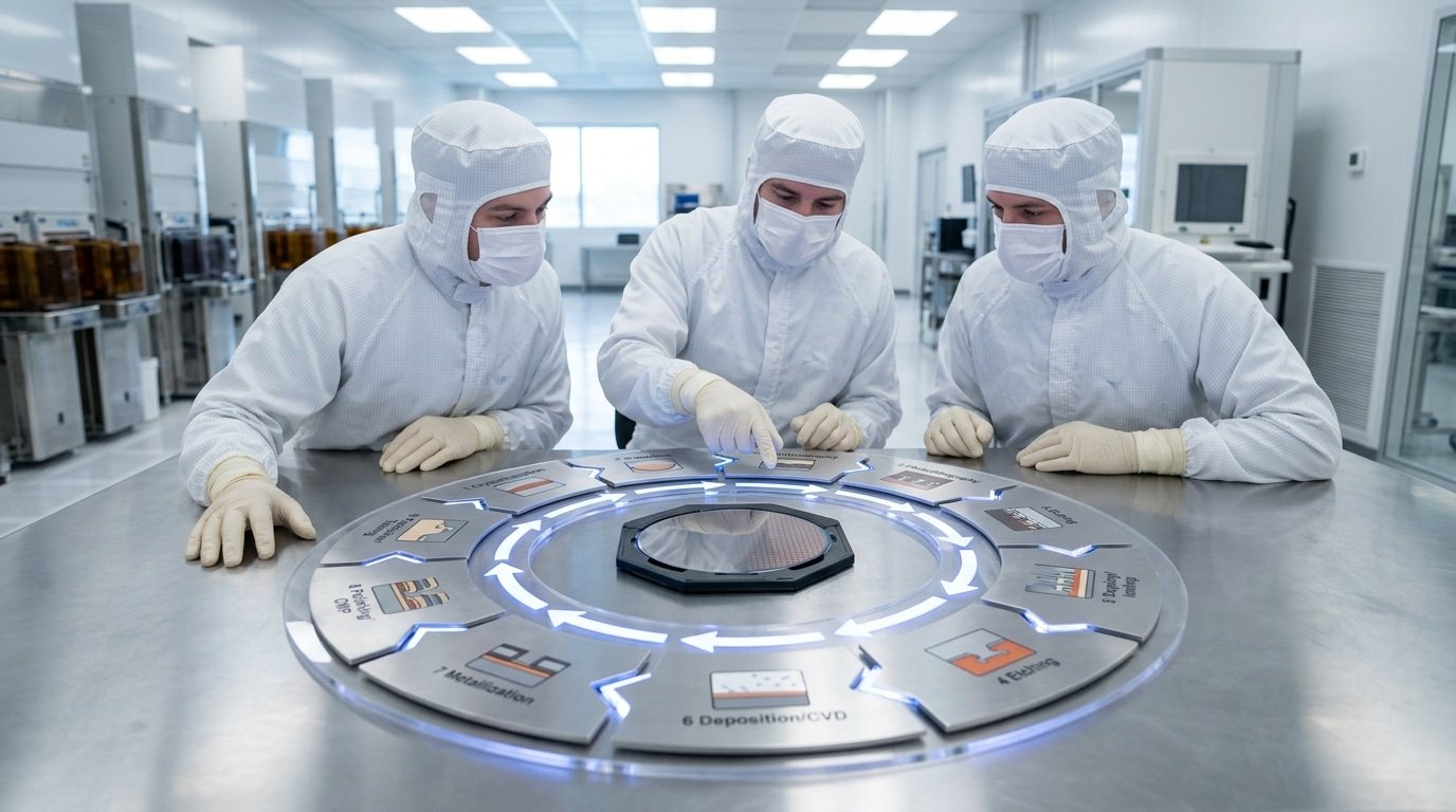
The semiconductor fabrication process steps span 9 core stages: wafer preparation, oxidation, photolithography, etching, doping, deposition, interconnect and CMP, wafer testing, and dicing and packaging. A modern logic chip can require over 1,000 individual operations and 80+ days inside the fab, according to industry data tracked through 2025. Stages 2 through 7 repeat in a loop rather than running once, with advanced chips needing 60 to 80 photolithography layers to build a complete circuit from a single polished silicon wafer.
Here is the short answer: making a single chip takes hundreds of operations, yet they all fall under 9 core phases. Wafer preparation comes first, then a repeating cycle of layering, patterning, and material change builds the circuit.
A modern logic chip can require over 1,000 individual process steps and 80+ days inside the fab, according to industry data tracked through 2025.
This guide breaks down each phase in plain terms, so you understand what actually happens to a wafer and why every step matters for chip performance.
Quick Takeaways
- Semiconductor fabrication spans 9 core stages, from wafer prep to packaging.
- Stages 2 through 7 repeat in loops, not a single pass.
- Advanced logic chips need 60 to 80 photolithography layers each.
- A modern chip requires 1,000+ operations and 80+ days inside fabs.
- CMP flattens each layer before the next patterning cycle begins.
The 9 Core Steps in the Semiconductor Fabrication Process at a Glance
The semiconductor fabrication process steps break down into nine core stages: (1) wafer preparation, (2) oxidation, (3) photolithography, (4) etching, (5) doping, (6) deposition, (7) interconnect and CMP (chemical mechanical polishing, which flattens each layer), (8) wafer testing, and (9) dicing and packaging.
Steps 2 through 7 repeat in a loop, not a single straight line.
Picture one polished disc of silicon entering the cleanroom. To turn it into working chips, the fab doesn’t run these stages once, it cycles them.
A modern logic chip can need 60 to 80 photolithography layers, and each layer pulls the wafer back through oxidation, lithography, etch, and deposition again.
This repeating “front-end” loop is the part people miss. Samsung notes that advanced logic lines use 300 mm silicon wafers running through hundreds of individual unit processes grouped into repeated cycles. Wikipedia sorts those many steps into four basic actions: deposition, removal, patterning, and modification.
The flow chart you see online looks linear, but the wafer physically loops the same tools dozens of times. Only the end stages, testing, dicing, packaging, happen once, at the “back end.”
A leading-edge chip can take roughly 26 weeks start to finish. We follow one wafer through all nine stages next.
Step 1 — Wafer Manufacturing and Surface Preparation
So here’s something wild. Every chip you’ve ever used basically starts out as sand.
The very first of the semiconductor fabrication process steps takes purified silicon and turns it into a mirror-flat approximately 300mm[1] disc, and it happens across four stages. There’s crystal pulling, slicing, polishing, and cleaning.
Mess this part up, and honestly, no amount of fancy patterning work later can rescue that wafer.
It all kicks off with the Czochralski method. Picture a tiny seed crystal dipping down into molten silicon sitting at approximately 1,414°C[2].
Then it slowly spins and gets pulled upward. The melt freezes onto that seed in perfect atomic order, and it grows into a single chunk of crystal up to 2 meters long and approximately 300mm wide.
Next, a diamond wire saw cuts the long crystal into thin discs, each one under 1mm[3] thick. After that comes chemical mechanical polishing, or CMP, which is essentially a slurry-and-pad process.
It grinds the surface down to a flatness measured in fractions of a nanometer. We’re talking smoother than a calm pond at the atomic scale.
Two real yield-killers are hiding here, though. Total thickness variation (TTV) measures how uneven a wafer is across its diameter.
When TTV runs high, it blurs the focus of the patterning work that comes later. Particle contamination is even worse.
A single 50-nanometer speck can short out a transistor completely.
So what’s the fix? RCA cleaning, which is a two-bath chemical wash that strips away organics and metal ions.
The final surface prep takes place inside a Class 1 ISO 14644-1 cleanroom. That room allows fewer than 10 particles per cubic meter, which is roughly 100,000 times cleaner than a hospital operating room.
These super-pure single-crystal discs then feed straight into oxidation and film deposition, which is what comes next.
Step 2 — Oxidation and Thin Film Deposition
After cleaning, the wafer grows or gains thin layers that insulate, protect, and conduct. Oxidation grows silicon dioxide directly from the silicon surface; deposition adds films from outside gases.
Both stages must hold film thickness uniform to within a few angstroms (1 angstrom = 0.1 nanometer), because that thinness sets the transistor’s threshold voltage, the exact gate signal needed to switch a chip on.
Dry vs Wet Thermal Oxidation
Thermal oxidation runs inside furnaces near 1000°C. Dry oxidation uses pure oxygen. It grows slowly but builds dense, high-quality gate oxides, the critical insulator under each transistor gate. Wet oxidation adds water vapor, growing thicker layers much faster for field isolation, where speed beats perfection.
The trade-off is simple: dry gives quality, wet gives speed. Fab engineers pick dry for the gate, wet for everything else.
Four Deposition Methods That Build the Stack
| Method | Full name | Best for | Typical use |
|---|---|---|---|
| CVD | Chemical Vapor Deposition | Thick dielectric films | Insulating layers between wires |
| PECVD | Plasma-Enhanced CVD | Lower-temperature films | Coatings over heat-sensitive metals |
| ALD | Atomic Layer Deposition | Atom-thin control | High-k gate dielectrics, barrier layers |
| PVD | Physical Vapor Deposition | Metal layers | Sputtering copper or aluminum |
ALD matters most at advanced nodes. It lays down one atomic layer per cycle, so a 30-angstrom barrier comes out within one or two atoms of target.
Thermo Fisher’s fabrication overview groups these as epitaxial and dielectric film deposition, among the primary categories of the semiconductor fabrication process steps.
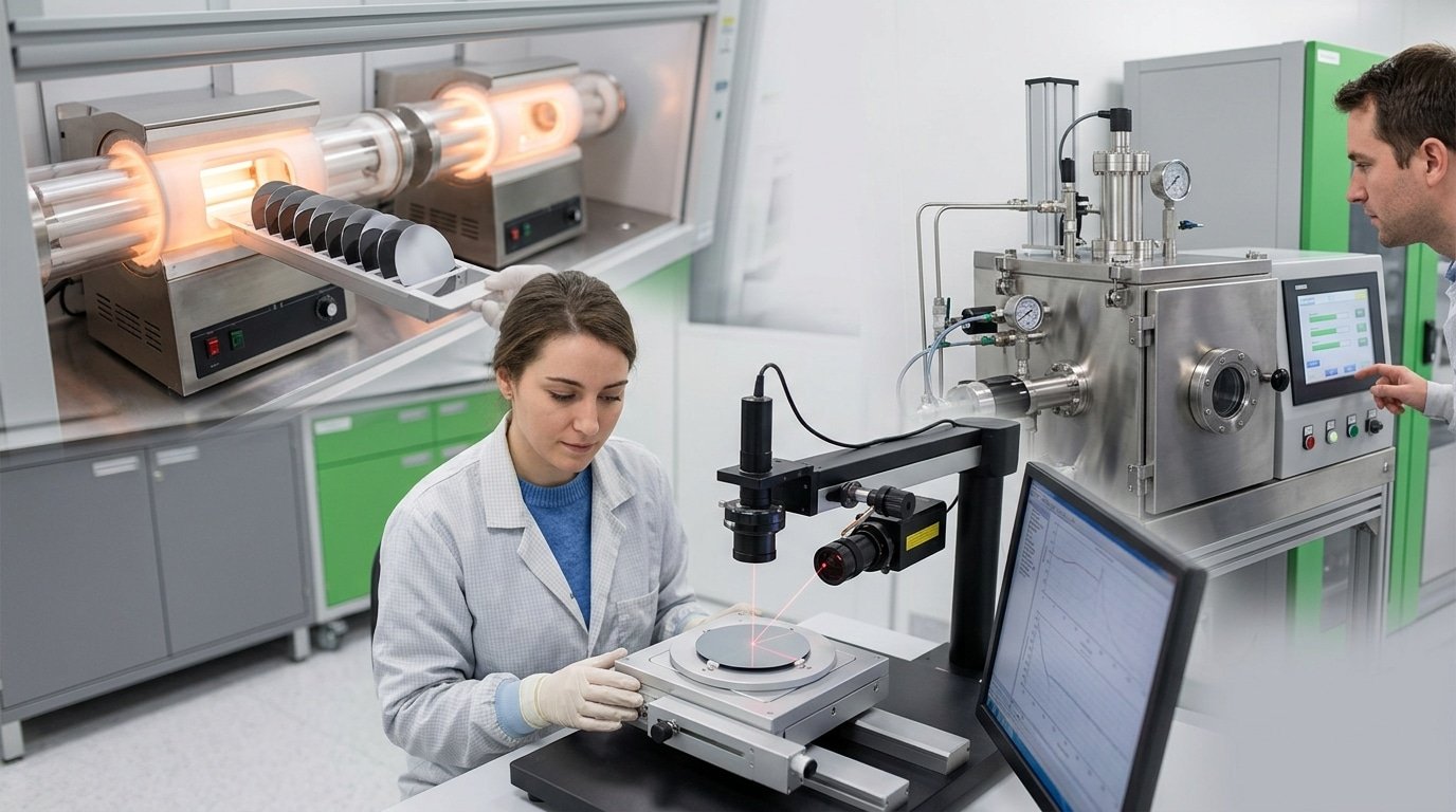
Fabs confirm thickness with ellipsometry, which measures how polarized light reflects off the film and bends, then back-calculates thickness within angstrom accuracy without touching the wafer. A 1-angstrom miss on a gate oxide can shift threshold voltage enough to fail a whole lot.
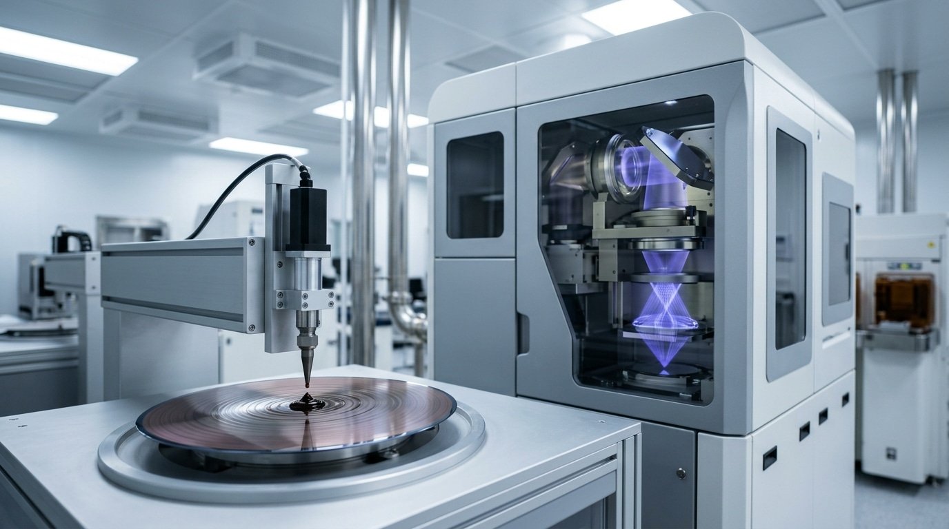
Step 3 — Photolithography and Photoresist Coating
Photolithography prints the circuit pattern onto the wafer. Think of it like a stencil that uses light instead of ink. A wafer gets coated, light shines through a patterned mask, and the parts that were exposed wash away once you develop them.
This is really the pattern-transfer heart of the semiconductor fabrication process steps. And it repeats dozens of times per chip.
The sequence moves fast and stays tight. First, a robot drops a liquid called photoresist, which is basically a coating that reacts to light, onto a spinning wafer turning somewhere between 1,000 and 4,000 RPM.
How fast it spins decides how thick the film ends up, and we’re talking accuracy down to a few nanometers. Then a soft bake near 90 to approximately 110 °C[4] cooks off the solvent so the resist firms up enough to hold an image.
Next comes alignment and exposure. The scanner lines up the new mask with the layers already on the wafer, fires the light, and prints the pattern. Wikipedia’s fabrication overview puts this whole stage under “patterning,” which is one of four core categories in chip making.
Two errors can quietly wreck how much usable material comes out:
- Overlay error, which happens when a new layer ends up even a few nanometers off from the layer beneath it. Vias that are out of place simply won’t connect.
- Critical dimension (CD) error, which shows up when a printed line comes out too wide or too narrow. Honestly, a drift of just 1 nm in CD can change how fast a transistor runs.
Here’s the brutal part. One defect in the mask repeats on every die across the reticle field. A scanner exposes many chips per shot, so a single bad spot can scrap hundreds of devices all at once.
EUV vs DUV Lithography and How Node Shrink Changes the Process
Direct answer: EUV uses 13.5nm light, while DUV immersion uses 193nm light. The shorter wavelength of EUV lets it print really fine features in just one go. The 193nm DUV, though, needs three to four exposure passes, something called multi-patterning, to reach the same tiny size.
And when you shrink things down from 7nm to 3nm, you basically multiply all these light-printing and etching loops, which adds cost and risk to the semiconductor fabrication process steps.
Wavelength matters here because light just can’t print features that are much smaller than its own size. So at 193nm, if you want to draw a 20nm line, you have to split one pattern across several masks and exposures.
That trick is what people call multi-patterning. And each time you split it, you’re adding another whole etching cycle.
| Metric | 193nm Immersion DUV | 13.5nm EUV |
|---|---|---|
| Wavelength | 193 nm | 13.5 nm |
| Numerical aperture (NA) | 1.35 | 0.33 (0.55 for High-NA) |
| Patterning passes per critical layer | 3–4 (quad-patterning) | 1 (single exposure) |
| Relative cost per layer | Lower per pass, higher total | Higher per pass, fewer passes |
A 5nm logic chip can actually require over 80 mask layers. And the most critical of those layers really decide whether DUV multi-patterning or EUV comes out ahead on cost.
ASML is the only company that makes EUV scanners, and they ship machines that weigh more than a school bus.
Here’s a practical tip, though. The people planning these factories keep track of “wafers per layer,” basically how much is produced per layer. Every extra DUV pass adds another chance for an overlay error, which is where the masks get misaligned and end up ruining the print.
Step 4 to Step 6 — Etching, Ion Implantation Doping and Layer Building
Etching carves the pattern into the wafer. Ion implantation shoots dopant atoms in to set electrical behavior. Annealing then heals the damage. These three semiconductor fabrication process steps repeat hundreds of times to stack the dozens of layers inside one chip.
⚠️ Common mistake: Assuming the 9 fabrication stages run once in a straight line. This happens because the “9 core steps” framing implies a single pass, but stages 2 through 7 actually repeat in loops—advanced logic chips need 60 to 80 photolithography layers, driving 1,000+ operations and 80+ days inside the fab. The fix: treat oxidation through CMP as a repeating cycle, where each completed layer is flattened before the next patterning round begins.
Two ways exist to remove material. Wet etch dunks the wafer in chemicals like hydrofluoric acid, cheap, but it etches sideways too, ruining tight features. Plasma or reactive-ion etch (RIE) uses charged gas to cut straight down. For sub-10nm features, only RIE delivers the vertical walls needed.
Watch for profile bowing, the etch eats out the middle of a trench wider than the top, like an hourglass. That short-circuits later metal fills. Engineers tune gas pressure and bias power to keep walls flat.
Implantation is precise atom injection. To make an n-type region (extra electrons), you fire phosphorus or arsenic; for p-type (electron holes), boron. Dose is measured in atoms per square centimeter, often 10¹³ to 10¹⁵.
The trap here is dopant channeling. If ions hit the crystal at the wrong angle, they slip between atom rows and bury too deep.
Fabs tilt the wafer about 7 degrees to scatter them. Then rapid thermal annealing (a approximately 1,000°C[5] flash for seconds) repairs the smashed lattice and locks dopants in place.
Step 7 to Step 8 — Interconnects, CMP and Why Each Step Repeats Hundreds of Times
After transistors are built, the chip needs wiring to connect them. Step 7 deposits copper interconnects using the damascene method.
Step 8 flattens the wafer with chemical-mechanical planarization (CMP) before the next layer goes down. These two steps then loop 10 to 20 times, which is why a “simple 6-step flow” never matches reality.
Copper damascene works backwards from old aluminum wiring. Instead of depositing metal then etching it, fabs etch trenches into insulation, fill them with copper, then polish away the excess.
Dual-damascene cuts both the wire trench and the via hole below it in one fill, saving a full deposition cycle per layer.
CMP is the unsung hero here. A spinning pad and chemical slurry grind the wafer flat to within a few nanometers, because each new metal layer needs a perfectly level base, otherwise the next lithography step loses focus across bumps and dips.
This stage is called back-end-of-line (BEOL). Advanced logic lines run through hundreds of individual unit processes on approximately 300mm wafers, with the litho-etch-CMP cycle repeating per layer. Skip the loop view, and you misjudge cost and cycle time badly.
In-Line Metrology and Defect Inspection Between Every Step
Fabs measure yield in real time using inspection stations placed between nearly every process step. Yield equals good die divided by total die on a wafer.
A defect density of 0.1 defects/cm² sounds tiny, but on a approximately 300mm[6] wafer with about 707 cm² of usable area, that means roughly 70 random killer defects scattered across the surface, enough to ruin dozens of chips.
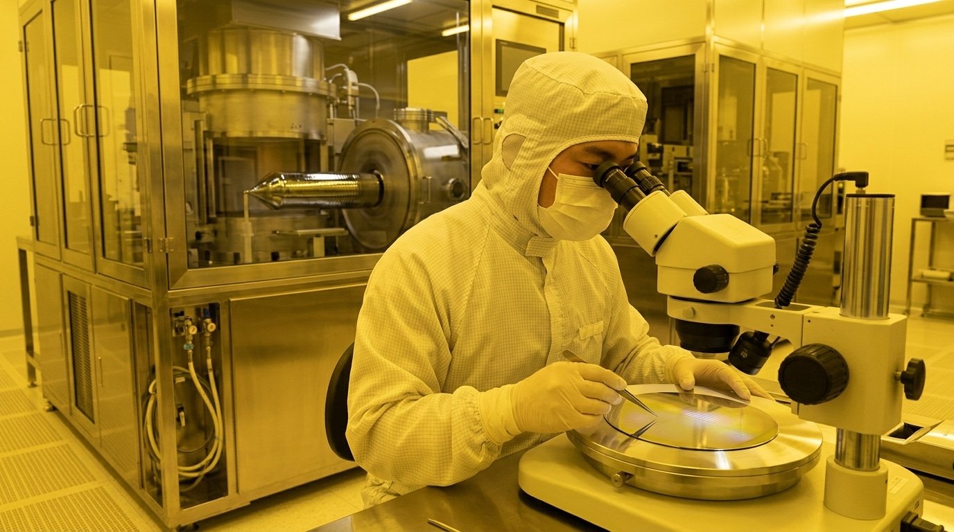
Two main tools catch these flaws. Optical inspection scans the wafer fast, comparing identical die to spot anything out of place.
E-beam inspection runs slower but resolves tiny defects below a few nanometers, the size that kills modern transistors. Scatterometry measures critical dimension (CD), the exact line width of a printed feature, by reading how light scatters off the pattern.
A metrology station sits after almost every step in the semiconductor fabrication process steps because a chip runs through hundreds of operations. Catching a misaligned layer early saves the wafer; catching it at final test wastes months of work.
Wikipedia’s semiconductor device fabrication entry notes fabs treat patterning and inspection as tightly linked.
Here is the math that scares engineers. If you’ve 200 small die on a wafer and 70 defects land randomly, your yield can drop below approximately 70%[7]. Each lost die at advanced nodes can cost over $10[8] in processing alone.
| Tool | What it measures | Speed |
|---|---|---|
| Optical inspection | Pattern defects, particles | Fast (full wafer) |
| E-beam inspection | Sub-nm killer defects | Slow, high resolution |
| Scatterometry | CD line width | Fast, non-contact |
Step 9 — Wafer Testing, Dicing and Advanced Packaging
The final stage of the semiconductor fabrication process steps tests every die on the wafer, cuts the wafer into individual chips, then seals each chip in a package that connects it to the outside world.
This back-end flow can take several weeks and adds approximately 30% or more to the total cost of advanced chips.
It starts with electrical wafer sort (EWS), also called probe testing. Tiny needles touch each die’s contact pads and run thousands of voltage and timing checks. Bad die get an ink dot or a digital flag. This screens out defects before any money is spent on packaging.
Next comes dicing. A diamond blade or laser cuts the wafer along thin “streets” between die. Laser dicing leaves narrower kerf (the cut gap), saving precious silicon on tightly packed wafers.
Then each die gets connected. Two methods dominate:
- Wire bonding — thin gold or copper wires link die pads to the package. Cheap and proven.
- Flip-chip — the die flips face-down onto solder bumps. Shorter paths mean faster signals.
High-end parts use 2.5D interposers and chip-on-wafer-on-substrate (CoWoS), where multiple chips sit on a silicon bridge. TSMC’s CoWoS packs CPU and high-bandwidth memory side by side, powering most AI accelerators in 2026. See Wikipedia on flip-chip bonding.
Last, burn-in testing runs chips hot under voltage for hours. This catches “infant mortality” failures, parts that work at first but die early, before they ever ship.
Common Misconceptions and Costly Mistakes in Reading the Fab Flow
The biggest myth? That a chip flows straight from step 1 to step 9 like a factory line.
It doesn’t. Real fabs loop the same photolithography, etch, deposition, and implant cycle hundreds of times.
Reading the flow as linear leads teams to underestimate cycle time and misplace where defects actually start.
Myth: one defect ruins one chip. In reality, a single contaminated tool can kill an entire field, the cluster of dies exposed in one lithography shot. A reticle defect repeats on every die it prints.
That’s why a missed particle costs far more than one chip’s worth of silicon.
Myth: smaller nodes mean fewer steps. The opposite is true. Advanced logic lines run through hundreds of individual unit processes on approximately 300 mm[9] wafers, and node shrink adds multi-patterning passes that multiply mask layers.
More steps means more cycle time, the full flow can stretch to about 26 weeks for advanced chips.
| Misconception | Fab reality | Cost impact |
|---|---|---|
| Flow is linear | Cycles repeat 100s of times | Cycle time underestimated by weeks |
| One defect, one chip | Reticle/tool defects hit whole fields | Yield loss across many dies |
| Smaller node, fewer steps | Multi-patterning adds mask layers | More steps, longer turnaround |
Practical tip: when reviewing a fab flow, track the layer count, not the step names. A 5nm logic chip can need 80+ mask layers, that number predicts cost and risk better than any block diagram.
Frequently Asked Questions
What are the steps in semiconductor device fabrication? The semiconductor fabrication process steps run as nine repeated stages: wafer prep, oxidation and deposition, photolithography, etching, ion implantation, layer building, interconnects with CMP, wafer testing, then dicing and packaging. Most steps loop many times before a chip is done.
Is Apple IDM, fabless, or foundry? Apple is fabless. It designs chips like the M-series and A-series but owns no fab; TSMC, a pure-play foundry, makes them. An IDM (integrated device manufacturer) like Intel designs and builds its own chips. A foundry only manufactures; a fabless firm only designs.
How long does a wafer take to fabricate? Front-end fab time runs 12 to 16 weeks for advanced logic. Counting design, masks, and back-end packaging, CubeFabs reports the full process can reach about 26 weeks for leading-edge chips. EUV layers add days each because of slow throughput.
Where can I find a process flow chart or PDF? For a clean reference, see Wikipedia’s Semiconductor device fabrication article, which groups every step into four categories: deposition, removal, patterning, and electrical modification. Foundry and equipment maker sites publish detailed flow diagrams too.
Key Takeaways and Next Steps for Going Deeper
The nine semiconductor fabrication process steps aren’t a straight line, they form a loop. Deposition, lithography, etch, and implantation repeat layer by layer until every transistor and wire is built.
A single approximately 300 mm logic wafer can run through hundreds of unit processes before it reaches packaging, as Samsung Semiconductor notes.
Read the whole flow through one lens: defects and yield. Every step adds risk, which is why metrology stations sit between cycles, catching particle defects and overlay errors before they multiply. A approximately 99%[10] per-step yield across 50 critical steps still drops final yield to roughly 60%.
Want to go deeper? Start with these one-source references:
- Process flow charts — Wikipedia’s four-category breakdown (deposition, removal, patterning, modification) gives a clean mental model.
- Foundry resources — Read TSMC, Samsung, and Intel technology pages for real node specs and unit-process counts.
- Metrology specs — Study overlay and critical-dimension tolerances published by tool makers like KLA and ASML.
Next move: pull up a detailed step diagram and trace one metal layer through its full deposit-pattern-etch-polish cycle. Seeing the loop in action makes the whole process click.
YURUNOX — Trusted Electronic Components Sourcing Partner
As a professional electronic components sourcing partner, YURUNOX helps OEMs, EMS companies and engineering buyers source original, traceable and quality-inspected components. Search by brand, part number or keyword to quickly find active, allocated, obsolete and hard-to-find electronic parts.
- ✔ Brand & Part Number Search
- ✔ Original & Traceable Components
- ✔ BOM Sourcing & RFQ Support
- ✔ Obsolete & Hard-to-Find Parts
References
- [1]asml.com
- [2]microchipusa.com
- [3]renesas.com
- [4]semiconductor.samsung.com
- [5]thermofisher.com
- [6]en.wikipedia.org
- [7]wevolver.com
- [8]cubefabs.com
- [9]power-and-beyond.com
- [10]screen.co.jp


