Standard 74HC CMOS logic ICs typically operate from a wide supply range of about 2 V[1] to approximately 6 V, making them work in both approximately 3.3 V and approximately 5 V systems (7400-series logic, Wikipedia).
That flexibility is exactly why picking the wrong part still trips up engineers every day.
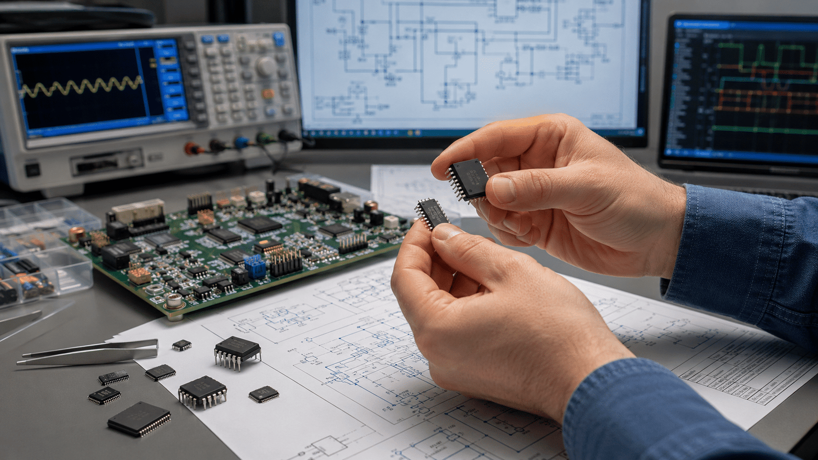
So how do you choose a logic IC? Match four things to your design: the logic family (speed and voltage), the supply voltage your board runs on, the output drive current your load needs, and the package that fits your assembly process.
Get those four right, and the part number almost picks itself.
This guide walks through each decision in order, voltage levels, propagation delay, fan-out, and footprint, with the real tradeoffs that datasheets bury and the mistakes that cause silent failures after the board ships.
Quick Takeaways
- Match the logic family to your supply rail before checking anything else.
- Use 74LVC (1.65–approximately 3.6V) for approximately 3.3V designs; 74HC (2–approximately 6V) for mixed rails.
- Verify propagation delay: 74HC runs 8–15ns, 74AC/74LVC hit 3–4ns.
- Check output drive current: 74HC sources 4–8mA, 74LVC handles ±24mA.
- Filter by voltage, speed, and package, then confirm a second source.
The Fast Answer for Choosing a Logic IC
Choosing a logic IC comes down to four checks, in order: match the logic family to your voltage rail, confirm the speed (propagation delay) is fast enough, verify the output can drive your load current, then make sure the part is actually in stock with a second source.
Get the voltage match wrong and nothing else matters.
Here is the workflow I run every time:
- Match the family to your rail. Running approximately 3.3 V? A 74LVC part operates from 1.65 V to approximately 3.6 V and talks directly to low-voltage microcontrollers, per NXP’s logic family data. Mixed approximately 3.3 V[2] and approximately 5 V? 74HC spans approximately 2 V to approximately 6 V, covering both rails (74HC reference).
- Check speed. General 74HC gates land around 8–15 ns delay at approximately 5 V. Need faster? 74AC and 74LVC drop to 3–4 ns.
- Verify drive current. Standard 74HC outputs source or sink roughly 4–8 mA per pin; 74LVC pushes ±24 mA. Read the VOH/VOL spec at your real load before committing.
- Confirm supply. Filter by voltage, speed, and package on a distributor parametric search, then pick a part with at least two manufacturers.
Propagation delay means the lag between an input changing and the output responding. Skip the brand loyalty. Pick the rail-matched family first, then narrow by the other three.

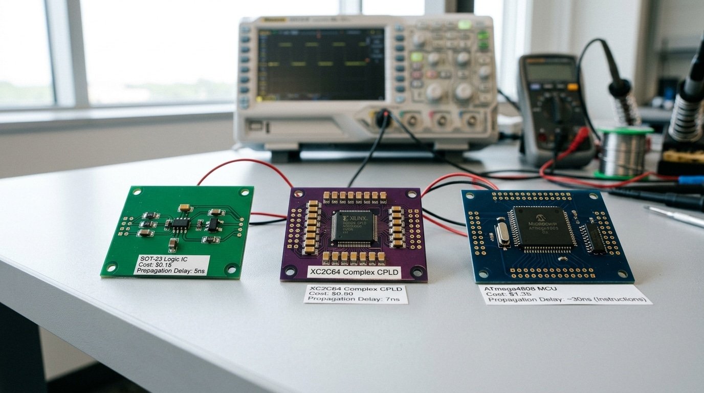
Discrete Logic Gates versus a CPLD, FPGA or Microcontroller
Before you spend an hour comparing part numbers, ask yourself one thing first. Do you actually need a standard logic IC at all?
If your job comes down to six or fewer simple functions, maybe a couple of NAND gates, an inverter, and one flip-flop, then a single 7400-style chip wins on cost, speed, and pure simplicity.
Once you go above that count, a CPLD or a microcontroller usually starts to pay off instead.
The math here is pretty blunt, honestly. A single 74HC00 quad NAND gate costs roughly $0.10 to $0.30 when you buy small quantities.
A small CPLD runs approximately $1 to $5, and a basic 8-bit MCU sits in a similar range. So for one or two gates, discrete logic ends up being 5 to 30 times cheaper.
Speed is really where discrete gates quietly dominate everything. A 74HC gate passes a signal through in about 8 to 15 ns at approximately 5 V, going by onsemi datasheet figures, and the faster 74AC or 74LVC families hit somewhere around 3 to 4 ns.
An MCU that reads one pin and writes another adds in delay from interrupts and clock cycles, often microseconds. That’s basically a 100x to 1000x penalty just for simple connecting logic.
So how to choose a logic IC versus programmable silicon? Honestly, just use this rule of thumb:
| Need | Best fit | Why |
|---|---|---|
| 1–6 fixed gates/functions | Discrete logic IC | Pennies, ~5–15 ns delay, no firmware |
| 7–50 functions, fixed behavior | CPLD | One chip, instant-on, predictable timing |
| State machines + I/O + compute | MCU | Flexible, but adds boot time and code |
Here’s one trap worth knowing. Never pick an MCU just to save a bit of board space. A single SOT-23 single-gate chip takes up under 3 mm², which is smaller than most MCU packages, and it has zero firmware you’ll ever have to maintain.
Start With Your Voltage Rail and Build the Decision Tree
Your supply rail picks the family before anything else does. A approximately 5V[3] board points you to HC, HCT, or LVC. A approximately 3.3V rail favors LVC or AHC. Drop to approximately 1.8V or below and AUP becomes the practical answer. Lock the rail first, then everything downstream gets simpler.
Why does the rail dominate? Because it sets which families even function. Standard 74HC CMOS logic runs from roughly 2V to 6V, so it spans both approximately 3.3V and approximately 5V systems. But 74LVC tops out at approximately 3.6V, feed it approximately 5V and you cook the part.
Here is the cascade I use when choosing a logic IC for a new board:
- Rail voltage → eliminates families that won’t tolerate your VCC.
- Target speed → if you need sub-5ns propagation delay, HC (8–15ns at approximately 5V) is already out; you move to AC, AHC, or LVC.
- Interface partner → does this chip talk to a approximately 3.3V MCU or a approximately 5V[4] sensor? That decides whether you need an LVC part with approximately 5V-tolerant inputs.
One concrete example: a approximately 1.8V microcontroller driving a sensor bus. AUP fits the rail at 0.8,approximately 3.6V and draws around 0.5 µA in standby. Try forcing HCT here and it simply won’t switch, HCT needs near-approximately 5V input thresholds. Three filters, one shortlist. That’s the whole method.

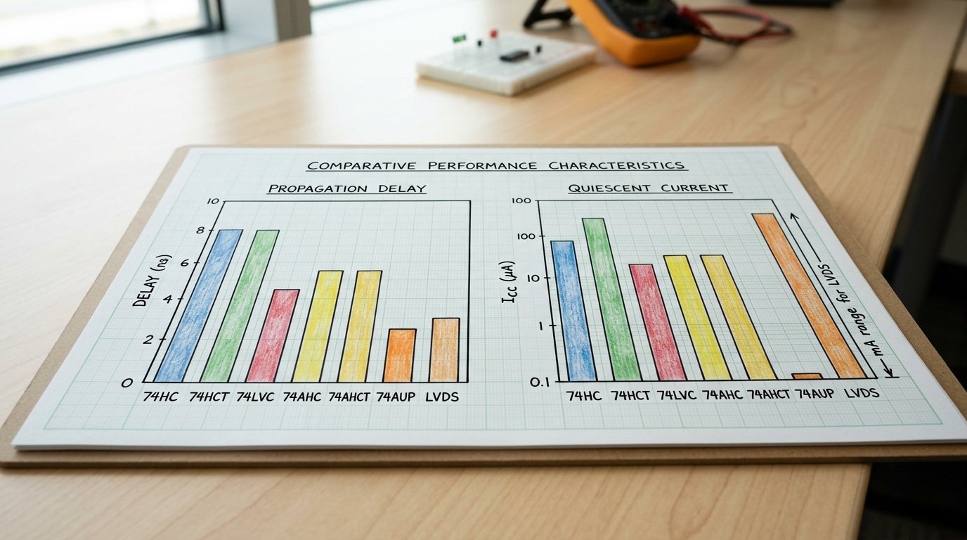
Comparing Logic Families With Real Numbers
Put the specs side by side and the choice gets obvious fast. LVC wins almost every approximately 3.3V bus job. AUP wins when battery life matters more than speed. Below are the real numbers that decide which family ends up on your board.
| Family | Supply range (V) | Typ. prop delay | Output drive | Quiescent ICC |
|---|---|---|---|---|
| 74HC | 2.0–6.0 | 8–15 ns @approximately 5V | ±4–8 mA | ~1 µA |
| 74HCT | 4.5–5.5 | 10–18 ns | ±4 mA | ~1 µA |
| 74LVC | 1.65–3.6 | ~3–4 ns | ±24 mA | ~10 µA |
| 74AHC | 2.0–5.5 | ~5 ns | ±8 mA | ~1 µA |
| 74AHCT | 4.5–5.5 | ~5 ns | ±8 mA | ~1 µA |
| 74AUP | 0.8–3.6 | ~4 ns | ±4 mA | ~0.5 µA |
| LVDS | 2.5–3.3 (rail) | ~0.3 ns skew | ~3.5 mA loop | varies |
Why does LVC dominate approximately 3.3V switching? Two reasons sit in the table. It runs from 1.65 V to approximately 3.6 V, so it talks straight to low-voltage microcontrollers, and its ±24 mA drive handles a loaded bus that HC (only ±4,8 mA at 4.5,5V) can’t push fast enough.
AUP plays a different game. With quiescent current near 0.5 µA and supply down to approximately 0.8V[5], it fits coin-cell wearables where a single gate runs for years. Knowing how to choose a logic IC means reading these four columns, not the family name.
One trap: 74HC propagation delay of 8,15 ns looks fine until your clock hits approximately 40 MHz, where a 25 ns period leaves no margin. Then LVC’s 3 ns is the only safe pick.
The 3.3V to 5V Compatibility Trap and Level Shifting
Connecting a approximately 3.3V part to a approximately 5V part fails silently more often than it works. The rule: a driver’s output HIGH (VOH) must clear the receiver’s input HIGH threshold (VIH), and the output LOW (VOL) must stay under VIL.
When you choose a logic IC for a mixed-rail board, check these four numbers before you wire anything.
Here is where it breaks. A approximately 3.3V CMOS output sits near 3.3V HIGH, well above the approximately 2.0V VIH that classic 74LS TTL treats as a valid HIGH.
So approximately 3.3V-to-approximately 5V often works one direction. The reverse doesn’t: a approximately 5V[6] output drives approximately 4V+ into a pure-CMOS approximately 3.3V input, exceeding its absolute maximum and stressing the gate.
| Path | Direct? | Why |
|---|---|---|
| approximately 3.3V CMOS → approximately 5V HCT input | Yes | HCT VIH is approximately 2.0V, so approximately 3.3V clears it |
| approximately 3.3V → approximately 5V HC input | No | HC VIH ≈ approximately 3.5V[7] (0.7×VCC); approximately 3.3V is borderline |
| approximately 5V → approximately 3.3V LVC input | Yes | LVC inputs are approximately 5V-tolerant |
| approximately 5V → approximately 3.3V HC input | No | Over absolute max; needs translator |
Two cheats save real money. HCT bridges approximately 3.3V-up-to-approximately 5V because its approximately 2.0V[8] threshold matches TTL.
And 74LVC tolerates approximately 5V on inputs while running off 1.65,approximately 3.6V, killing approximately 5V-down-to-approximately 3.3V signals safely. When neither fits, use a dedicated bidirectional translator.
A TXS0108E costs roughly $0.50 in volume versus a failed board respin worth thousands.
Reading the Datasheet Parameters That Actually Decide Selection
Five numbers settle most logic IC choices: propagation delay (tpd), drive current (IOH/IOL), input capacitance (Cin), supply current (ICC), and the recommended operating conditions table. Everything else is detail. Read these first and you skip half the part comparisons.
Propagation delay is the gap between an input edge and the matching output edge. General-purpose 74HC parts sit around 8,15 ns at 5 V, while 74AC and 74LVC drop to 3,4 ns.
For a approximately 50 MHz bus, your clock period is 20 ns, a 15 ns gate eats most of your timing budget. Pick the faster family.
Fan-out tells you how many inputs one output can drive. The math is simple.
Take the output drive, a 74HC pin sources or sinks roughly 4,8 mA at 4.5,5 V, then divide by the input current each load draws.
CMOS inputs pull almost nothing in DC, so the real limit is capacitive: each input adds about 3,5 pF, and ten loads means 30,50 pF hanging on one driver, which slows your edges and stretches tpd.
Check VOH and VOL at your actual load current, not the headline number. A part rated 8 mA may only guarantee approximately 3.84 V output high at that current, borderline for a approximately 5 V receiver.
ICC matters for battery work: CMOS idles near 1 µA, while old bipolar TTL pulls milliamps doing nothing.
When you ask how to choose a logic IC for a tight design, treat the recommended operating conditions block as a hard fence, not a suggestion.
Package, Pin Count and Thermal Constraints for Your Board
The package decides how the part gets soldered, how much board space it eats, and whether you can fix a bad joint by hand. So part of knowing how to choose a logic IC is matching the package to your assembly reality, not just the schematic.
Going from a through-hole DIP to a tiny leadless package can shrink the footprint by more than 90%[9]. That density helps, but it punishes rework.
| Package | Pin pitch | Assembly fit | Hand-rework reality |
|---|---|---|---|
| DIP-14 | approximately 2.54 mm | Prototype, breadboard | Easy with any iron |
| SOIC-14 | approximately 1.27 mm | Low-density SMT | Hand-solderable |
| TSSOP-14 | approximately 0.65 mm | Mid-density SMT | Needs flux + fine tip |
| SC-70 (5-lead) | approximately 0.65 mm | Single-gate, dense | Hot air, hard by hand |
| SOT-23 (5/6-lead) | approximately 0.95 mm | Single-gate logic | Doable with steady hands |
Single-gate packages like SC-70 and SOT-23 hold one or two gates, so you place logic exactly where you need it instead of routing signals across the board to a shared 14-pin chip. That saves trace length on a approximately 3.3V bus.
Tiny packages hide a thermal limit. An SC-70 has a junction-to-ambient thermal resistance near 350,450 °C/W.
At fast toggle rates, dynamic power (P = C × V² × f) climbs, and a part switching a heavy load at tens of MHz can heat up fast. Vendors like Texas Instruments publish max power dissipation curves per package, check them before pushing a single-gate part hard.
Availability, Second Sources and Long-Term Supply Risk
A perfect part from one supplier is still a risk. If that vendor stops making it, your board stops shipping. So part of knowing how to choose a logic IC is checking that at least two makers build a drop-in equivalent before you commit the footprint.
Start with lifecycle status. Every distributor flags a part as Active, NRND, or Obsolete.
NRND means “Not Recommended for New Designs”, the maker still sells it but plans to kill it. Picking an NRND part for a product you’ll build for five years is asking for a redesign mid-stream.
The good news: mainstream 74-series logic is the safest bet in the catalog. The standard 7400-series logic family has been in production since 1966 and stays in volume manufacture through 2026.
A 74HC00 quad NAND gate ships from Texas Instruments, Nexperia, Onsemi, and Diodes Incorporated, four independent fabs building the same pinout.
That cross-vendor overlap is your safety net. Here’s what to verify before locking a part:
- Two or more active sources for the exact pinout and package — not just the function
- No NRND or PCN flag (a Product Change Notice signals a pending move or end-of-life)
- Standard JEDEC package like SOIC or TSSOP, which any maker can second-source
One pitfall I see in BOM reviews: engineers pick a clever multi-function part from a single niche vendor to save one package. When that part hit a 40-week lead time during the 2021,2022 chip shortage, those boards sat unbuilt.
A pair of basic 74LVC gates would have shipped the whole time.
Skip the exotic single-source part. Pick the boring 74-series equivalent with four fabs behind it.
Common Mistakes That Wreck a Logic IC Selection
Four mistakes ruin more logic IC designs than any datasheet error: floating CMOS inputs, missing bypass caps, mismatched thresholds between families, and overloading one output. Each one shows a clear symptom on a scope. Learn to read those symptoms and you save hours of blind probing.
Floating CMOS inputs. An unused gate input left unconnected drifts to the threshold voltage and the input stage oscillates. On a scope you see ringing on the supply rail and the gate output jittering at megahertz.
The chip also gets warm. TI’s application notes warn that floating inputs cause excess supply current and oscillation.
Fix: tie every unused input to VCC or GND through a resistor. Never leave it open.
No bypass cap. Skip the decoupling capacitor and switching outputs yank the ground reference up and down, called ground bounce. The scope shows a 200,500 mV spike on GND each clock edge, and downstream logic misreads it.
Standard practice is a 0.01 µF to 0.1 µF cap right at the VCC,GND pins of each IC. Place it within a few millimeters, not across the board.
Mixing families with marginal thresholds. A 74LS output rated VOH of approximately 2.4 V driving a CMOS input that wants approximately 70%[10] of VCC sits in the forbidden zone. The scope shows a slow, rounded edge that never reaches a clean HIGH.
The gate draws milliamps fighting the ambiguous level. Check VOH against VIH before you commit.
Over-fanning one output. A 74HC pin sources only 4,8 mA. Hang ten high-current loads on it and edges slow, levels sag, and the part overheats. Knowing how to choose a logic IC means budgeting fan-out per output, not after the schematic is done.
Frequently Asked Questions
Short, direct answers to the questions designers ask most when picking a part.
How do you choose a logic IC in general?
Work in this order: match the logic family to your supply rail, confirm input thresholds line up across connected parts, check propagation delay and drive current against your load, then pick a package your line can solder.
Vendor design guides from Renesas list the same six parameters as the deciding factors.
Is the 7400 still commonly used?
Yes, but rarely the original bipolar 74-series. The modern equivalent is 74HC00 or 74LVC00. The 74HC family runs from about 2 V to 6 V, per Wikipedia, so one part covers both approximately 3.3 V and approximately 5 V boards. Designers reach for these for glue logic and quick fixes.
What does the 7420 do?
The 7420 holds two independent 4-input NAND gates in one 14-pin package. Each gate outputs LOW only when all four inputs are HIGH. Tie any unused inputs to VCC or GND, never floating.
How do you spot a bad logic IC?
Use a meter first. A dead part often draws milliamps of static current instead of the ~1 µA a healthy CMOS gate idles at. On a scope, watch for ringing, stuck outputs, or rise times slower than the datasheet’s 8,15 ns spec for 74HC.
Putting Your Logic IC Selection Workflow Into Practice
Run every part through the same five steps, in order, and you’ll rarely pick wrong. The rail decides the family.
The family decides your speed and drive headroom. The interface decides whether you need level shifting.
Then you confirm the package fits and check that two suppliers stock it. That sequence is the whole answer to how to choose a logic IC without backtracking.
Keep this checklist beside your schematic:
- Lock the rail. approximately 3.3V points to LVC (approximately 1.65V–3.6V). approximately 5V points to HC (approximately 2V–6V). A approximately 1.8V domain points to AUP.
- Set the speed budget. HC gives 8–15 ns; AC and LVC give 3–4 ns. Pick the slowest part that meets timing — slower edges mean less ringing.
- Check the interface. Driver VOH must clear receiver VIH at the load current. Mismatch means a shifter.
- Fit the package. Match pad pitch to what your assembly line can place.
- Verify two sources. No second source, no design-in.
Lock the actual part using distributor parametric search, filter by voltage, channel count, speed, package, and temperature. Then pull the datasheet from the maker’s library and confirm VOH/VOL at your real load before you commit.
One last move. Build the gate on a breadboard, tie unused inputs to VCC or GND, and watch the output on a scope before you route a single trace. Five minutes there saves a board respin.


