The lead time for custom chip manufacturing typically runs 26 to 52 weeks from final design sign-off to packaged parts, stretching to 12–18 months for a leading-edge ASIC. During 2025 peak demand, mature nodes at TSMC and Samsung pushed past a full year.
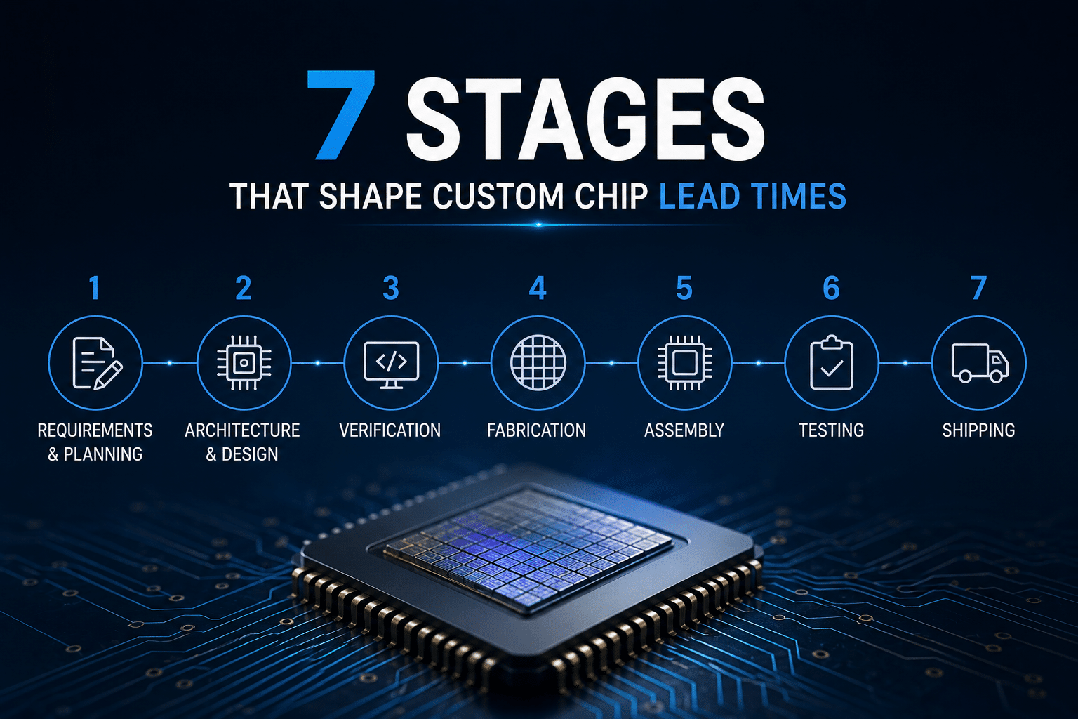
Delays rarely come from the fab itself; they accumulate across seven stages—design/RTL, verification, tape-out and mask, NRE setup, wafer fabrication, packaging, and test—where a single bottleneck can add months to the schedule.
That gap between “tape-out” (when your design files go to the foundry) and a working chip in hand decides whether your product ships on schedule or slips two quarters.
Most delays don’t come from the fab itself. They pile up across seven distinct stages, design verification, mask production, wafer fabrication, packaging, and testing among them, where a single bottleneck can add months.
Below, each stage gets broken down with real timelines and the choices that move the clock.
Quick Takeaways
- Custom chip lead times run 26–52 weeks; leading-edge ASICs take 12–18 months.
- Track all seven stages—delays usually accumulate outside the fab itself.
- Run verification (12–24 weeks) in parallel with design to save time.
- Budget approximately $1M–$50M for NRE setup fees on advanced process nodes.
- Avoid peak demand periods when mature nodes can exceed full-year waits.
The 7 stages that shape custom chip lead times at a glance
The lead time for custom chip manufacturing runs 12 to 18 months for a leading-edge ASIC (application-specific integrated circuit, a chip built for one job). That clock spans seven phases: design/RTL, verification, tape-out and mask, NRE setup, wafer fab, packaging, and test plus qualification.
Each phase hands off to the next, so a slip in one shifts everything downstream.
Here is how the months split across the chain:
- Design / RTL — writing the logic in code, 8 to 16 weeks.
- Verification — proving the logic works before you spend on masks, 12 to 24 weeks, often overlapping design.
- Tape-out and mask — locking the final layout and cutting the photomasks, 6 to 12 weeks.
- NRE setup — non-recurring engineering, the one-time fees and process prep that can hit approximately $1M–$50M on advanced nodes.
- Wafer fab — the actual silicon, 10 to 20 weeks of cleanroom cycle time.
- Packaging and assembly — 4 to 10 weeks.
- Test and qualification — burn-in and reliability checks, 6 to 16 weeks.
The single longest pole is usually wafer fabrication. A 5nm flow at TSMC needs 1,000+ process steps, and queue time alone can rival actual fab time when capacity is tight.
Skip the guesswork on dates. Verification, not fab, is what blows most schedules, a single missed corner case sends you back for a respin, adding 3 to 6 months and a fresh mask bill. Plan buffers there first.
The stages below break each phase into week-ranges you can drop straight into a Gantt chart.
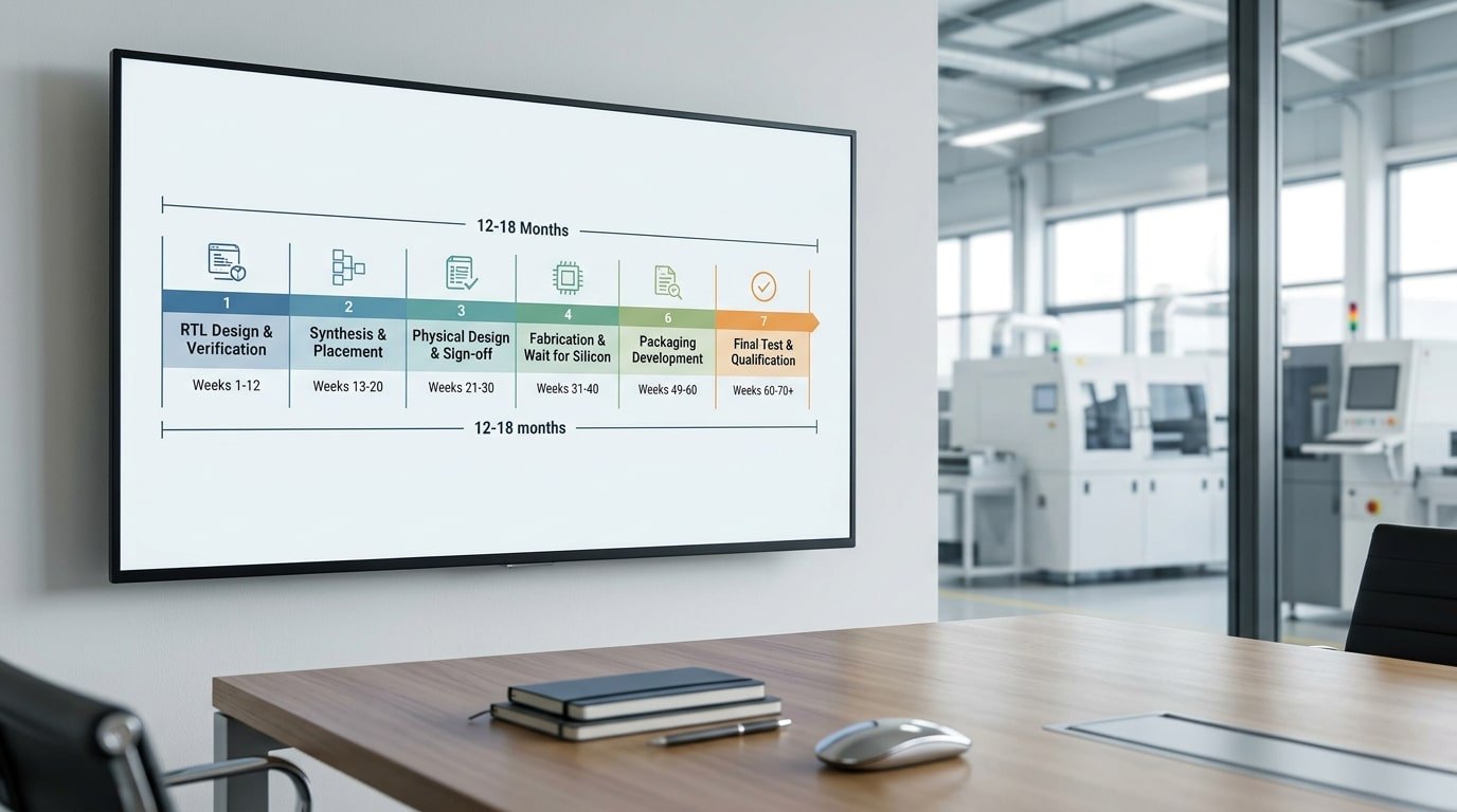
Stage-by-stage week-range table from RTL freeze to qualified parts
So picture this. From RTL freeze, which is basically the moment your Verilog code gets locked down and nobody can change the design anymore, all the way to having finished parts in your hands, you’re looking at 38 to 70 weeks for a leading-edge design.
The table below breaks that whole span out across all seven phases.
Here’s the thing though. Stages that run one after another add up directly. The ones that overlap only count once.
| Stage | Week range | Runs serial or parallel |
|---|---|---|
| Front-end design & verification | 8–20 | Serial (gates everything after) |
| Physical design & tape-out prep | 6–12 | Serial, partly overlaps verification |
| Mask set fabrication | 4–8 | Serial after tape-out |
| Wafer fabrication | 10–16 | Serial after masks ship |
| Packaging & assembly | 3–6 | Serial, but tooling builds in parallel |
| Test program development | 6–10 | Parallel with fab and packaging |
| Reliability qualification | 6–12 | Serial after first packaged parts |
Now here’s the trap I’ve watched most buyers fall right into. They add up every single row.
But test program development actually runs at the same time as wafer fab, so its 6 to 10 weeks usually just vanish into the rest of the schedule.
That’s exactly why a simple sum of 43 to 84 weeks shrinks down to roughly 38 to 70 weeks of real lead time for custom chip manufacturing.
Reliability qualification is the one stage you really can’t run alongside anything else. JEDEC standards like JESD47 require burn-in and temperature cycling on actual packaged units.
So this clock only starts ticking once your first silicon comes back. Older, more mature designs (28nm and above) often land near the low end.
Advanced ones push toward the high end.

Front-end design and verification queue before tape-out
Front-end work is the single widest swing in the lead time for custom chip manufacturing. This phase runs two months for a small block and six months for a complex SoC. Verification iterations, not design itself, cause most of the variance.
Front-end means everything before tape-out (the moment you send final design files to the foundry). It splits into four stages: RTL design, synthesis, physical checks, and timing closure.
- RTL design — writing the chip logic in Verilog or VHDL. RTL means register-transfer level, a code description of how data moves between memory and logic.
- Synthesis — software turns that code into a gate-level netlist (a map of actual transistors and wires).
- DRC/LVS — Design Rule Check confirms shapes obey foundry spacing rules. Layout-versus-Schematic confirms the layout matches the netlist.
- Timing closure — making sure signals arrive on time at every clock edge across all temperature and voltage corners.
Verification eats the schedule. Functional verification alone consumes roughly 60% of total project effort, according to the Siemens EDA Wilson Research industry surveys. Each bug found in a UVM testbench triggers a fix, re-simulation, and re-check loop. One missed corner case can add weeks.
Complexity drives the timeline hard. Three factors stretch it most:
- Block count — a 50-block SoC needs far more integration testing than a 5-block design.
- Third-party IP — licensed cores like PCIe or DDR controllers need integration and re-verification, often adding three to four weeks each.
- Mixed-signal content — combining analog and digital circuits requires extra co-simulation that pure digital chips skip.
One practical tip: lock your verification plan before writing RTL, not after. Teams that define coverage goals upfront close timing weeks faster than teams that bolt testing on late. This phase feeds directly into tape-out and mask set fabrication.

Tape-out, mask set fabrication, and NRE turnaround
Tape-out adds another 4 to 10 weeks to the lead time for custom chip manufacturing. Most of that time gets eaten up waiting in line at the mask shop and building the set of photomasks, which are basically the stencils used to print the chip design.
The clock really starts ticking the moment you hand off the GDSII file. Think of that file as the final blueprint database. It tells the factory exactly where every tiny transistor and wire is supposed to sit.
But before any glass actually gets carved up, the layout has to go through something called mask data prep, or MDP. This step applies optical proximity correction, which essentially bends and reshapes the design slightly so it prints correctly, considering that light tends to bend around really small features.
For a 5nm design, the MDP work alone can take 2 to 3 weeks. And that is just pure computing time running across huge banks of servers.
Then you get to the physical mask set itself. Each chip needs one photomask for every layer in the process.
At the most advanced nodes, like 5nm and 3nm, that adds up to 30 to 80-plus reticle layers. Why so many?
Because some features are too small to make in a single exposure, so they get split across several steps using multi-patterning. Every single extra layer is one more quartz plate.
And each one is written by an electron-beam tool that can cost approximately $50,000 or more for the critical masks.
This is exactly why non-recurring engineering costs, or NRE, blow up at the leading edge. A full 5nm mask set runs approximately $15 to 20 million, according to industry mask cost data. Compare that to roughly $1 million back at 28nm. Quite a jump, honestly.
So here is the real tradeoff you face. Pay extra for a priority slot and your mask set cuts the line, with turnaround dropping from 8 weeks down to 4.
But that rush fee can tack on another approximately 20% to your NRE. Skip the rush instead, and you simply wait behind everyone else’s jobs.
Practical tip: Lock your GDSII clean before you submit. A single OPC re-spin restarts the whole queue clock. That alone burns another 3 to 5 weeks.
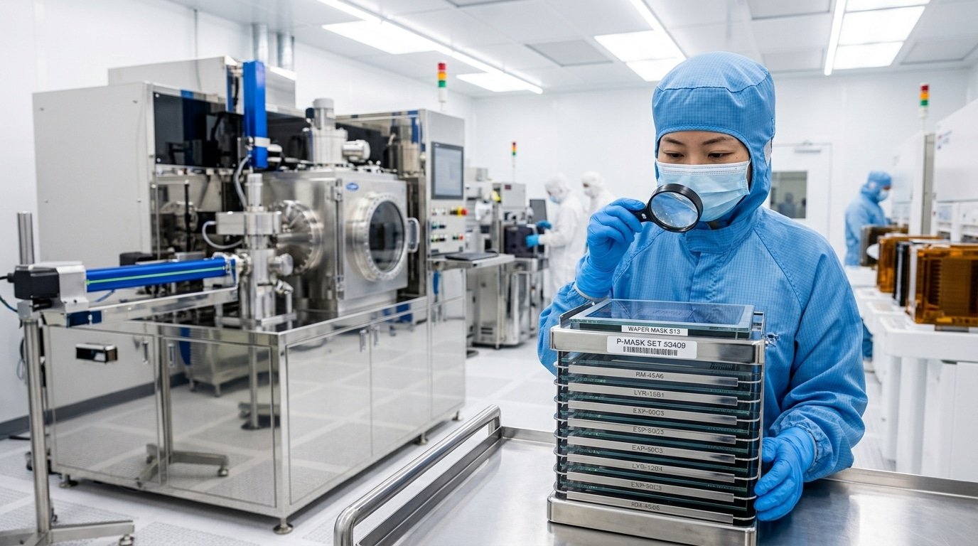
Wafer fabrication queue times and the cleanroom cycle
Wafer fabrication splits into two clocks: raw process time of 12 to 16 weeks, plus a queue wait of 0 to 8 weeks before your lot even starts. That queue is the wildcard in the lead time for custom chip manufacturing.
Your wafers can sit in a foundry holding area for weeks while higher-priority lots run first.
Raw process time is the physical work. A leading-edge wafer passes through 800 to 1,200 process steps, including photolithography (printing circuit patterns with light), etching, ion implantation, and deposition.
Each layer must finish before the next begins. At advanced nodes like 5nm, that stacking pushes physical cycle time to roughly 16 weeks.
You can’t rush this part. The chemistry takes the time it takes.
The queue is where foundry choice bites. When a fab runs near full capacity, your “lot start” date slides.
TSMC reported capacity utilization above approximately 90% through 2025, so non-priority customers waited weeks longer to begin. GlobalFoundries, focused on mature nodes like 12nm and 22nm, often carries more open capacity for specialty work.
| Foundry path | Typical node | Queue + raw cycle |
|---|---|---|
| TSMC, peak loading | 5nm / 7nm | 4-8 wk queue + 16 wk run |
| GlobalFoundries specialty | 12nm / 22nm | 1-3 wk queue + 12 wk run |
One insider tip: ask your foundry for a “hot lot” or priority run. It can cut cycle time by 30 to approximately 50% but costs a steep premium per wafer. Book your slot at tape-out, not after. Capacity allocation closes fast.
How process node and foundry choice shift mask and fab timelines
Your node choice can swing the lead time for custom chip manufacturing by six months or more. A mature 28nm part at GlobalFoundries or SMIC skips the slowest queues.
A 3nm part at TSMC waits behind EUV lithography (extreme ultraviolet light that prints the tiniest features) and capacity that’s booked solid.
The split comes down to two things: how many photomask layers your design needs, and how full the fab’s most expensive tools are.
| Node | Typical foundry | Mask set cost | Mask layers | Fab queue (weeks) |
|---|---|---|---|---|
| 65nm | SMIC / GF | approximately $200K–$400K | ~30 | 2–4 |
| 28nm | GlobalFoundries | approximately $1M–$2M | ~40 | 4–8 |
| 7nm | TSMC | approximately $5M–$9M | ~60 | 8–14 |
| 5nm / 3nm | TSMC | approximately $15M–$30M+ | 80+ | 14–24 |
Why does EUV stretch timelines? Each EUV layer runs on ASML’s EUV scanners, and there are only a few hundred of these machines worldwide.
A 5nm design uses many EUV layers, so it competes for scarce tool hours. A 28nm part uses none.
That single fact explains most of the gap.
The CHIPS Act is shifting this math. New US fabs like TSMC Arizona and Intel’s Ohio sites are adding domestic leading-edge capacity through 2026.
Practical tip: if your part qualifies for a mature node, lock it there early. You skip the EUV bottleneck entirely and shave 8 to 12 weeks off your schedule.
Packaging, assembly, and test qualification at the back end
The back end adds 6 to 16 weeks to the lead time for custom chip manufacturing, and most buyers forget to budget it. After wafers leave the fab, they still need dicing, packaging, and a full test program before you hold a sellable part.
Skip this math and your launch date slips by a quarter.
Three jobs happen here. First, dicing cuts the wafer into individual dies with a diamond blade or laser. Then assembly bonds each die into a package. Finally, every unit runs through a test program that checks if it actually works.
Package choice drives the clock. Plain wirebond (thin gold wires connecting die to pins) is the cheapest and fastest.
Flip-chip flips the die onto solder bumps for better speed. Advanced 2.5D/3D packaging stacks multiple dies on a silicon interposer,think of it as a tiny circuit board between chips.
That interposer alone can add 6 to 12 weeks at an OSAT (outsourced assembly and test house).
| Package type | Typical back-end time | Best for |
|---|---|---|
| Wirebond | 3–5 weeks | Low-cost, low-pin-count parts |
| Flip-chip | 5–8 weeks | High-speed logic, GPUs |
| 2.5D/3D stacked | 10–16 weeks | AI accelerators, HBM memory |
Reliability qualification eats the rest. HTOL (High Temperature Operating Life) bakes parts at approximately 125°C while running them,the standard JEDEC JESD22-A108 test runs approximately 1,000 hours, roughly 6 weeks. Temperature cycling swings parts between hot and cold to find cracks. These run in parallel, but a single fail forces a re-spin.
One practical tip: book your OSAT slot at tape-out, not at wafer-out. Advanced packaging queues for HBM-class designs have stretched past 12 weeks since 2025 due to AI demand. This stage connects directly to the compression levers covered next.
Levers to compress lead time without blowing the budget
You can cut the lead time for custom chip manufacturing by 3 to 6 months without doubling your spend, if you pick the right lever for your volume. The four proven moves are shuttle runs, multi-project wafers (MPW), second-source packaging, and die buffers.
Each trades one resource (money, control, or risk) for calendar weeks.
A shuttle run, or MPW, is when many designs share one mask set and one wafer. Instead of paying full mask cost, often approximately $1M+ at advanced nodes, you rent a small block of silicon.
Europractice publishes fixed MPW calendars across many nodes. The catch: you ride the fab’s schedule, not yours.
Miss a deadline and you wait weeks for the next slot.
| Lever | Time saved | Tradeoff | Best for |
|---|---|---|---|
| MPW / shuttle run | Skips dedicated mask queue; cuts cost 60–approximately 90% | Locked to fab calendar; tiny die count | Prototypes, first silicon |
| Second-source packaging | 4–8 weeks off back-end queue | Requires dual qualification effort | High-volume parts |
| Long-lead die buffer | Removes 12–16 week refab wait | Capital tied up in inventory | Steady production demand |
| Early reticle reservation | 2–4 weeks off tape-out wait | Deposit forfeited if you slip | Firm tape-out dates |
Stack levers by stage. Use an MPW for your first prototype, then book a dedicated mask once the design is stable.
For production, qualify two assembly houses early, a single back-end vendor is the most common single point of failure in chip schedules. Buffering 8 to 12 weeks of long-lead wafers smooths demand spikes without the full refab penalty.
Common timeline mistakes buyers make when planning a tape-out
The biggest planning mistake is treating the fab cycle as the total lead time for custom chip manufacturing. Buyers see “12 to 16 weeks of wafer processing” and build a schedule around it.
But fab time is maybe approximately 30% of the clock. Front-end design, mask delays, packaging, and qualification eat the rest.
Plan only for fab, and you miss your launch by a year.
The second trap is assuming first-pass silicon will work. It often doesn’t. Industry data from Synopsys functional verification surveys has long pegged first-pass silicon success near 30%, meaning roughly 7 in 10 designs need at least one re-spin (a redesign and second tape-out to fix bugs).
Here is what a re-spin does to your calendar. Say bring-up finds a logic bug in week 60. You fix the RTL, re-verify, order a new mask set, and re-run the fab and back end:
- RTL fix and re-verification: 3 to 6 weeks
- New mask set (or partial metal-layer mask): 4 to 8 weeks
- Second fab and assembly cycle: 8 to 12 weeks
That adds 3 to 5 months to a project most people budgeted as a single straight line. A metal-only re-spin (changing just wiring layers, not transistors) is cheaper and faster, but you still wait for the back end again.
Two more errors sink schedules. Underbudgeting qualification means teams skip burn-in and reliability stress, then fail an automotive AEC-Q100 audit late.
And booking fab capacity too late pushes you behind other customers in the queue. Lock your wafer slot 4 to 6 months before tape-out, and carry a re-spin buffer in every plan.
Frequently asked questions about custom chip lead times
Short answers to the questions buyers ask most, with real numbers attached.
How long does it take to make a semiconductor chip?
For a custom leading-edge ASIC, plan on 12 to 18 months from RTL freeze to qualified parts. A mature-node design with a proven IP block can land in 8 to 12 months.
Pure wafer fab time inside the cleanroom is only 12 to 16 weeks of that, the rest is design, mask making, packaging, and test.
Are mature nodes faster than leading-edge?
Yes, and by a wide margin. A 28nm or 40nm mask set ships in about 4 weeks, while a 3nm or 5nm extreme ultraviolet (EUV) mask set can take 10 weeks or more.
Mature lines also carry less queue pressure, so the total lead time for custom chip manufacturing often drops by three to six months on a planar node.
How do MPW shuttles affect timing?
A multi-project wafer (MPW) shuttle, where many designs share one wafer to split mask cost, saves money but adds calendar time. You wait for the next shuttle slot, which runs on a fixed schedule.
Some advanced-node shuttles run only every 6 to 8 weeks, so a missed slot can push your prototypes back two months.
Does the CHIPS Act change domestic lead times?
The 2022 CHIPS Act committed approximately $52.7 billion to U.S. fab construction. New plants from TSMC Arizona and Intel Ohio add domestic capacity, which should ease queue waits over time. But fabs ramp slowly, most won’t hit full volume until 2026 to 2028, so near-term lead times stay tight.
Putting your custom chip timeline together
Stack all seven stages and a leading-edge ASIC lands at 12 to 18 months from RTL freeze to qualified parts. Build your schedule by adding each stage’s worst-case range, then add a buffer for one re-spin.
Engage your foundry and OSAT (the outsourced assembly and test house that packages your die) before front-end design ends, not after.
Use this planning checklist before you commit to a launch date:
- Front-end design and verification — 16 to 40 weeks. Lock RTL only when coverage hits approximately 95%+.
- Tape-out and mask set — 4 to 10 weeks. Confirm your slot before GDSII handoff.
- Wafer fabrication — 12 to 16 weeks raw, plus queue.
- Packaging and assembly — part of the 6 to 16 week back end.
- Test qualification — runs concurrent where possible.
- Foundry and OSAT slot booking — book 3 to 6 months ahead.
- Re-spin buffer — add 12 to 20 weeks.
Why the buffer matters: a 2024 Siemens EDA report found roughly 75% of designs require at least one re-spin before they ship. A second mask set and fab cycle alone adds three to four months. Plan for it, or your launch date is fiction.
The single highest-use move is early engagement. Booking foundry capacity and locking your OSAT during verification, not after tape-out, can shave 6 to 8 weeks off queue time. Foundries reserve hot-lot slots for committed customers first.
Ready to map your own dates? Download our custom chip planning template to plug in your node, package, and re-spin assumptions, or book a consult with a design-services partner to pressure-test your schedule before you sign a foundry contract. See TSMC’s dedicated foundry services for current engagement models.
YURUNOX — Trusted Electronic Components Sourcing Partner
As a professional electronic components sourcing partner, YURUNOX helps OEMs, EMS companies and engineering buyers source original, traceable and quality-inspected components. Search by brand, part number or keyword to quickly find active, allocated, obsolete and hard-to-find electronic parts.
- ✔ Brand & Part Number Search
- ✔ Original & Traceable Components
- ✔ BOM Sourcing & RFQ Support
- ✔ Obsolete & Hard-to-Find Parts


