Electronic chips are made by purifying silicon from quartz sand, growing it into crystal ingots, slicing those into thin wafers, and then layering billions of microscopic transistors through repeated patterning, etching, and material deposition before testing and packaging. The full process spans over 1,000 separate steps and can take more than 3 months. It all happens inside cleanrooms kept thousands of times cleaner than a surgical operating room, since a single dust speck smaller than a bacterium can ruin an entire batch.
According to Wikipedia’s overview of semiconductor device fabrication, the whole thing “uses a multiple-step process including thermal oxidation, thin-film deposition, ion implantation, and etching to build circuits on a single-crystal silicon wafer.”
So how are electronic chips made, really?
Here is the short version. Raw silicon gets purified into a crystal, then it is sliced into thin discs called wafers.
After that, billions of tiny transistors are layered onto it through repeated rounds of patterning, etching, and adding small amounts of other materials. And then it is tested, cut apart, and sealed into the finished package that you would find tucked inside your phone or laptop.
The 9 steps below will walk you through that exact journey, starting from a chunk of material made from sand all the way to a working chip that is ready to be shipped out. Each stage really builds on the one before it.
And honestly, a single speck of dust, smaller than a bacterium, can ruin the entire batch.
Quick Takeaways
- Chip fabrication spans 1,000+ steps and takes three to four months.
- Cleanrooms stay thousands of times cleaner than surgical operating rooms to prevent contamination.
- A single dust speck smaller than a bacterium can ruin entire wafer batches.
- Nine core steps transform quartz sand into a packaged, working CPU.
- Process includes thermal oxidation, thin-film deposition, ion implantation, etching, and final packaging.
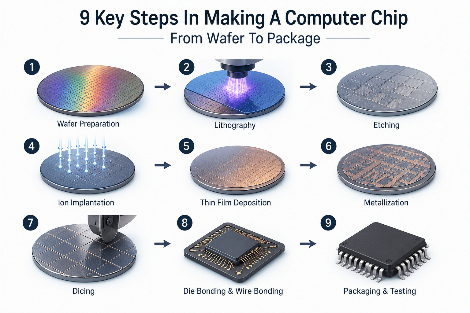
How A Computer Chip Goes From Sand To Package In 9 Steps
A computer chip starts as ordinary quartz sand and ends as a packaged CPU through 9 major steps: purifying silicon, growing crystal ingots, slicing wafers, building oxide and film layers, patterning with light, etching transistors, wiring with metal, testing, and packaging.
The full trip can take up to about four months from design sign-off to finished chips, and may run through hundreds of individual process steps.
So how are electronic chips made in practice? Picture a single transistor, one tiny switch, smaller than a virus.
To build it, fabs (chip factories) stack 30 or more functional layers on a silicon wafer using repeated cycles of three core moves: depositing thin films, patterning them with light, and etching away the excess.
This article traces that one chip from sand to socket. At each step, we put numbers on the cost, time, and difficulty, why a approximately 300mm[1] wafer holds hundreds of dies, why most fail before shipping, and why a single fab costs approximately $10,20 billion to build.
Here is the 9-step map you’ll follow:
- Refine sand into ultra-pure silicon ingots
- Slice, lap, and polish the wafer to a mirror finish
- Grow oxide layers and deposit thin films
- Pattern circuits with EUV photolithography
- Etch and dope to form transistors
- Add metal interconnect wiring
- Test the wafer for working dies
- Dice the wafer into individual chips
- Package and run final tests
Each step builds on the last. Skip the explanations of yield and cost, and the rest of chipmaking never makes sense.
Step 1 Refining Sand Into 99.9999999% Pure Silicon Ingots
Every chip starts out as quartzite sand, but the silicon inside has to hit approximately 99.9999999% purity, nine nines, written as 9N. Basically that means fewer than one foreign atom for every billion silicon atoms.
At that level of cleanliness, a single stray boron or phosphorus atom sitting in the wrong spot can flip how a transistor behaves and completely kill the device.
The whole journey actually starts in an arc furnace. Workers heat quartzite alongside carbon at roughly 2,000°C[2] to make rough silicon, which comes out around 98% pure.
And honestly, that is nowhere near good enough. The silicon reacts with hydrogen chloride to form trichlorosilane gas, which then gets distilled over and over again. After that it gets laid back down as super clean polysilicon rods.
This one step alone strips out most of the metal contaminants.
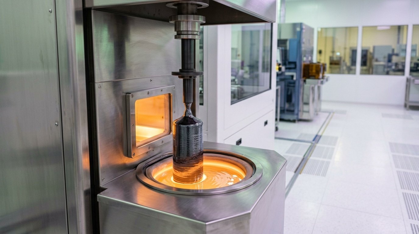
Then comes growing the crystal. In the Czochralski process, the polysilicon melts down inside a quartz container.
A tiny seed crystal dips into the molten pool and slowly gets pulled upward while it spins. The atoms freeze onto that seed in perfect alignment, essentially forming one continuous single crystal.
What you end up with is a cylinder shaped ingot up to 300mm (30cm) in diameter, which is the standard wafer size for modern chip factories.
This is slow work, really. Pulling a full approximately 300mm ingot can take a whole day or even longer, because rushing it introduces flaws called dislocations that wreck the crystal order.
Understanding this purity step is key to grasping how are electronic chips made, since every later step assumes a flawless crystal base.
One practical note from the industry. The quartz container itself slowly dissolves oxygen into the melt. Engineers manage this carefully, because trace oxygen actually changes how the wafer handles later heat steps.
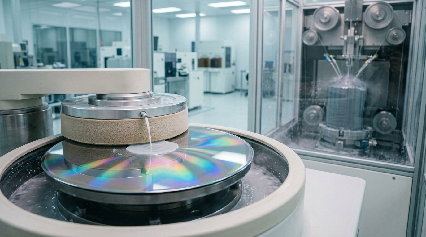
Step 2 Slicing, Lapping, And Polishing The Silicon Wafer
The cylindrical silicon ingot from Step 1 gets sliced into razor-thin discs called wafers. Each wafer is about 0.775 millimeters thick, roughly the width of eight stacked sheets of paper.
A single approximately 300mm[3] wafer can later hold hundreds of finished chips, so any flaw here multiplies across every die on the surface.
A diamond wire saw does the cutting. Picture a single strand of wire, coated in diamond grit, sawing back and forth thousands of times.
The wire is thinner than a human hair, which keeps “kerf loss”, the silicon wasted as dust during each cut, to a minimum. Even so, a meaningful slice of expensive purified silicon ends up as sawdust.
Slicing leaves the wafer rough and slightly bent. Two cleanup steps fix that:
- Lapping — abrasive slurry grinds both faces flat and removes saw damage.
- Edge grinding — rounds the wafer rim so it doesn’t chip or crack during later handling.
The final and most demanding step is chemical-mechanical polishing (CMP). A spinning pad plus a chemical slurry buffs the surface to a mirror finish, flat to within a few nanometers across the entire approximately 300mm disc.
Understanding this matters when you study how electronic chips are made, because the next steps print features smaller than a virus. A bump of even a few nanometers can ruin the focus of the lithography light, turning good silicon into scrap.
That’s why surface defects cascade into yield loss. As ingots reach 300mm diameters (2023 data from imec), one scratch can spoil multiple chips at once. Fabs measure flatness obsessively here, a polishing error costs more than the wafer itself.
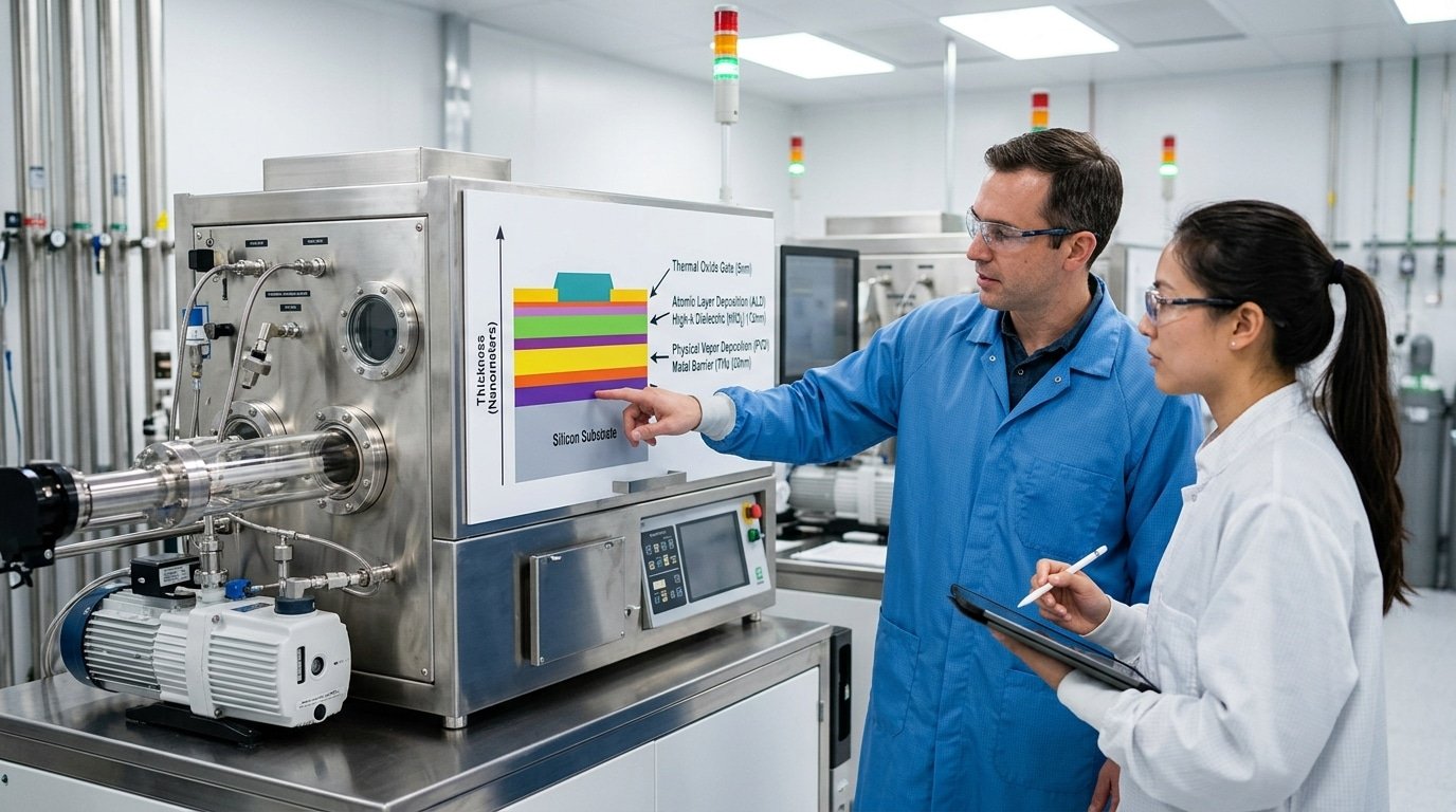
Step 3 Growing Oxide Layers And Depositing Thin Films
Once the polishing is done, that plain silicon wafer gets covered with layers that either block electricity or carry it. Some of these layers are only a few atoms thick.
Engineers really have two ways to put these films down. One is thermal oxidation, which bonds oxygen right into the silicon surface, and the other is deposition, which lays material from the outside onto the wafer.
Getting a handle on this layering is basically central to how are electronic chips made.
Thermal oxidation is the easiest one to picture. The wafer simply sits inside a furnace heated to somewhere between 800 and 1,200°C while oxygen or steam reacts with the silicon underneath.
What grows is a glassy silicon dioxide layer that works as the insulator for the transistor’s gate. How thick that film ends up depends on how long it cooks and how hot it gets.
Modern gates can be under 2 nanometers thick, which is roughly 10 silicon atoms stacked one on top of another.
Deposition takes care of everything oxidation simply cannot do. Three methods really lead the field here.
- CVD (Chemical Vapor Deposition) — gases react on the hot wafer surface and leave behind a solid film. This one handles the thicker insulating and polysilicon layers.
- ALD (Atomic Layer Deposition) — adds one single atomic layer with each cycle. It’s slow but incredibly precise. This is what builds the ultra-thin high-k gate insulators that took over from silicon dioxide once chips dropped below 45nm.
- PVD (Physical Vapor Deposition) — sprays metal atoms onto the wafer to form barrier and seed layers, basically prepping the surface before the copper wiring goes in.
The genuinely hard part is keeping things even. A film has to vary by less than a few atoms all the way across a approximately 300mm wafer. Otherwise the transistors at the edge will act differently from the ones in the center.
Even the smallest shift in gas flow or temperature can cause defects. According to Wikipedia’s fabrication overview, these cycles of deposition, oxidation, and etching repeat across 30 or more functional layers in an advanced chip.
Each layer stacks on the one below it with almost no room for mistakes.
Here’s one practical thing I’ve picked up. Fabs run plain test wafers every single day and measure film thickness using ellipsometry before they ever risk a real production wafer. If you catch a 1nm drift early, you scrap one test wafer instead of a approximately $50,000[4] batch.
Step 4 Photolithography And Mask Patterning With EUV Light
Photolithography is basically how they print the circuit blueprint onto the wafer. First the wafer gets coated with something called photoresist, which is really just a liquid that reacts to light. Then they shine light through a mask that holds the pattern they want.
After that, a developer chemical washes away the parts of the resist that got exposed, and what’s left behind is a precise stencil. This one step actually decides how small the transistors can be. And it repeats dozens of times for every single chip.
So how are electronic chips made small enough to pack billions of transistors into them? Honestly, the whole answer comes down to wavelength.
The older tools used to rely on ultraviolet light at 193nm. But to shrink the features down below 7 nanometers, the industry had to switch over to extreme ultraviolet light, often shortened to EUV, which sits at a 13.5nm wavelength.
Shorter light just prints finer lines, kind of the same way a sharp pencil draws thinner marks than a fat crayon does.
And EUV is brutally hard to work with. The light gets absorbed by both air and glass, so the entire system has to run inside a vacuum and uses curved mirrors instead of regular lenses.
The light itself is generated by blasting tiny tin droplets with a laser around 50,000 times every second, which is wild when you think about it.
Only one company, ASML over in the Netherlands, actually builds these machines. A single EUV scanner costs more than $150 million, weighs around 180 tonnes, and ships in roughly 40 freight containers. No competitor has managed to match it so far.
That kind of monopoly really gates the whole industry. A fabrication plant simply can’t make the most advanced chips, like the processors inside Apple or NVIDIA products, without having ASML tools.
The pattern alignment has to hit nanometer accuracy, so the wafers end up passing through lithography 30 or more times as each new layer stacks on top of the one before it.
Pro tip: overlay error, which is basically the misalignment between layers, ruins way more chips than most people would expect. Engineers track it down to fractions of a nanometer, because one shifted layer is enough to kill the entire die.
Step 5 Etching And Ion Doping To Build The Transistors
After photolithography prints the pattern, etching carves it into the wafer, and ion doping injects impurities to form working transistors.
💡 Counterintuitive: Making a single chip takes over 3 months and 1,000+ separate steps—not the fast, automated stamping most people imagine. Evidence: each wafer cycles repeatedly through thermal oxidation, thin-film deposition, ion implantation, and etching inside cleanrooms thousands of times cleaner than surgical operating rooms, where one dust speck smaller than a bacterium can destroy an entire batch worth millions.
Plasma etching uses charged gas to remove exposed silicon and oxide with atomic precision, while ion implantation fires boron or arsenic atoms into the silicon to create the electrical regions that switch a transistor on and off.
Here is how the layers actually get cut. The patterned photoresist acts like a stencil.
Plasma, a glowing cloud of reactive ions, bombards the surface and strips away material only where the resist leaves it bare. This is called anisotropic etching, meaning it cuts straight down, not sideways.
That vertical control matters. A 3-nanometer transistor gate can’t have sloped walls, or the chip leaks current.
Once the trenches and gates are shaped, doping begins. A transistor needs three parts:
- Source and drain — the two ends current flows between, doped to be N-type (extra electrons) or P-type (missing electrons).
- Gate — the switch that controls whether current passes.
- Channel — the silicon path under the gate.
To make N-type silicon, machines implant phosphorus or arsenic, which add free electrons. For P-type, they implant boron, which creates “holes” where electrons are missing.
Place an N region next to a P region and you get a junction, the basic on/off gate of every transistor. Understanding how electronic chips are made comes down to this: a chip is billions of these tiny N-P junctions wired together.
Why does doping precision decide switching speed? The implant dose controls how easily electrons move.
Too few dopant atoms and the transistor switches slowly. Too many and it leaks power when it should be off.
Engineers control this to within a few percent across the entire wafer. Modern fabrication repeats thermal oxidation, thin-film deposition, ion implantation, and etching dozens of times to stack every layer of a chip.
A practical detail few people know: after implantation, the silicon crystal is damaged. The boron and arsenic atoms crash in and knock silicon atoms out of place.
So the wafer goes through rapid thermal annealing, heated to around 1,000°C for a few seconds. This heals the crystal and locks dopants into position.
Skip it, and the transistor never works right.
This step is where a flat sheet of silicon becomes a living circuit. The same etching and doping cycle, repeated across a approximately 300mm[5] wafer, builds tens of billions of transistors on a single chip, each one switching billions of times per second.
Steps 6 To 9 Metallization, Testing, Dicing, And Packaging
After transistors are built, four final stages turn bare silicon into a working CPU: metallization wires the transistors together, wafer probe testing screens for defects, dicing cuts the wafer into chips, and packaging seals each chip for use.
Understanding these last stages is key to how electronic chips are made and shipped.
Step 6: Copper Interconnect Metallization
A single transistor does nothing alone. It needs wiring. Metallization stacks 15 or more layers of copper interconnects above the transistors, each connected by tiny vertical plugs called vias. Copper replaced aluminum around 1997 because it carries current with less resistance.
The numbers are staggering. A single advanced chip can hold packed into a fingernail-sized area. Engineers use a damascene process: etch trenches first, fill them with copper, then polish the surface flat before adding the next layer.
Step 7: Wafer Probe Testing
Before cutting anything, testers check every die on the wafer. A probe card lowers hundreds of fine needles onto each die’s contact pads and runs electrical tests in seconds.
Bad dies get an ink dot or a digital flag so they’re scrapped later. This step catches defects early, saving the cost of packaging chips that will never work.
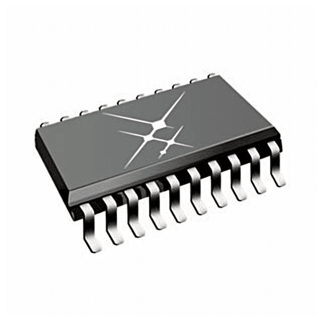
Steps 8 And 9: Dicing And Packaging
A diamond saw or laser slices the wafer into individual dies along thin streets between them. Each good die then gets attached to a substrate, wire-bonded or bump-bonded for electrical connection, and sealed in a protective package.
- Wire bonding: ultra-thin gold or copper wires link die pads to the package leads.
- Flip-chip bonding: tiny solder bumps flip the die face-down onto the substrate for faster signals.
- Encapsulation: epoxy or a metal lid shields the die from moisture and physical damage.
The whole journey, from design sign-off to volume chips, can take up to about four months. After packaging, a final test confirms each CPU meets its speed and power targets before shipping.
Why Yield Loss Means Many Chips On Every Wafer Fail
Yield is the percentage of working chips on a finished wafer. When a new chip first enters production, yield often sits at approximately 50% or lower, meaning half the dies are dead before they ship.
As engineers fix problems, yield climbs over months toward approximately 80% or higher. Understanding yield is central to how electronic chips are made, because it decides whether a fab earns money or burns it.
The killer is defect density, the number of flaws per square centimeter of silicon. A single dust particle smaller than a bacterium can short a transistor and ruin one die.
That’s why fabs run cleanrooms with fewer than 1 particle per cubic foot, cleaner than a hospital operating room by a factor of thousands. Learn more about cleanroom classification standards.
Math makes this brutal. A approximately 300mm wafer holds hundreds of dies.
If defect density is 0.1 defects per cm², a large approximately 600mm[6]² die fails far more often than a tiny approximately 50mm² one, bigger chips catch more random dust. This is why GPUs, with huge die sizes, yield worse than small mobile chips.
How Binning Saves Failed Premium Chips
Not every flawed die gets thrown away. After wafer testing, chipmakers sort dies by performance in a process called binning.
A high-end CPU with one bad core gets disabled and sold as a cheaper 6-core model instead of a 8-core. A chip that fails at approximately 5GHz but runs stable at approximately 4GHz[7] ships as a lower-clocked part.
- Full pass: sold as the flagship product at top price.
- Partial defect: bad cores disabled, sold as a mid-tier chip.
- Speed-limited: stable only at lower clock, sold as a budget model.
- Dead die: scrapped — pure loss.
This salvage strategy is why a approximately $300 and a approximately $600 chip can come from the same wafer. The hundreds of process steps behind every wafer, and the up to four months it takes to reach volume production, per ASML, mean each scrapped die wastes real money.
Binning recovers some of that loss by matching imperfect silicon to cheaper price tiers.
Practical insight: mature nodes like 28nm hit yields above approximately 90%[8] because their defects are well understood. Brand-new nodes like 2nm start far lower, which is one reason chips cost so much when they launch.
Why A Single Chip Fab Costs $10-20 Billion To Build
A leading-edge chip fab costs approximately $10,20 billion because it stacks the world’s most expensive machines inside the world’s cleanest building, and runs both nonstop for years. EUV scanners alone run roughly $200 million each, and a single fab needs a fleet of them.
That price wall is why understanding how electronic chips are made also means understanding who can afford to make them.
Start with the building. A cleanroom rated Class 1 holds fewer than one dust particle per cubic foot of air, millions of times cleaner than a hospital operating room. One stray speck ruins a chip, so the fab pumps and filters air constantly.
The scanners are the real budget killer. ASML’s most advanced EUV lithography machines cost over $150 million each, weigh as much as two Airbus A320 jets, and ship in roughly 40 freight crates. A fab buys dozens.
Then come the utilities. A single advanced fab can drink 10 million gallons of ultrapure water per day, enough for tens of thousands of homes, and pull hundreds of megawatts of power, the load of a small city.
TSMC, Samsung, and Intel are essentially the only firms that can fund this scale, plus the 3-to-5-year build timeline before the first wafer ships.
That economics chokepoint shapes global supply: when one fab stumbles, the whole world waits.
Which Countries And Companies Actually Make The Most Chips
Taiwan dominates advanced chip manufacturing. TSMC alone controls over 60%[9] of the global foundry market and makes more than 90% of the world’s most advanced chips, the 5nm and 3nm logic used in iPhones, AI accelerators, and high-end CPUs.
South Korea, the US, China, and Japan fill out the rest of the supply chain.
Here’s the key split most people miss: making chips and designing chips are separate businesses. The same multi-step process, photolithography, deposition, etching, and packaging, explains how electronic chips are made everywhere, but only a handful of fabs can run it at the cutting edge.
| Player | Role | Standout fact |
|---|---|---|
| TSMC (Taiwan) | Pure-play foundry | ~approximately 60%+ foundry share; leads 3nm production |
| Samsung (South Korea) | Foundry + memory | Largest maker of DRAM and NAND flash memory |
| Intel (US) | Integrated maker | Builds fabs in Arizona and Ohio under the US CHIPS Act |
| SMIC (China) | Foundry | China’s largest foundry; restricted from EUV tools |
| ASML (Netherlands) | Tool supplier | Sole maker of EUV lithography machines |
One company makes every machine that prints the smallest features: ASML. No EUV scanner, no advanced chip. That single chokepoint is why governments fight over export rules.
The geography is dangerously concentrated. Most leading-edge fabs sit within a few hundred miles of Taiwan and South Korea, a region exposed to earthquakes and political tension.
The US passed a approximately $52 billion CHIPS Act in 2022 specifically to pull some of that capacity back home, and Japan offered subsidies to bring TSMC to Kumamoto. Even so, building a fab takes years, so the concentration won’t ease before the late 2020s.
Practical takeaway: when you read that a phone uses a “3nm chip,” it almost certainly rolled off a TSMC line in Taiwan, even if a US company designed it.
Frequently Asked Questions About How Chips Are Made
Quick answers to the questions people ask most about how electronic chips are made, from the metals inside them to how long the whole process takes.
How do chips get so incredibly small?
Chips shrink because light prints features smaller than a virus. Extreme ultraviolet (EUV) light has a wavelength of just 13.5 nanometers, letting fabs draw transistor parts only a few atoms wide. A single fingernail-sized chip can pack tens of billions of these transistors today.
What metals and elements go into a chip?
The base is purified silicon, refined to approximately 99.9999999% purity. On top of that, manufacturers add:
- Copper — the main wiring metal since the late 1990s, replacing aluminum for faster signals.
- Gold — used in wire bonds that connect the chip die to its package, prized for not corroding.
- Boron and arsenic — implanted as dopants to create the positive and negative regions inside transistors.
- Tungsten and cobalt — fill tiny vertical holes that link wiring layers.
An advanced chip can hold tens of miles of microscopic metal wiring stacked across more than 30 layers.
How long does the full process take?
Far longer than most people guess. Building a finished wafer takes around 12 to 14 weeks of nonstop processing.
Counting design sign-off through volume production, the timeline can stretch to about four months across hundreds of individual steps, according to ASML. A wafer may pass through the same lithography tool dozens of times.
Where can I find accurate step-by-step videos or documentaries?
Skip the flashy clips with wrong narration. For trustworthy explanations of how electronic chips are made, watch ASML’s official process videos, Intel’s “From Sand to Silicon” series, and Asianometry’s deeply researched breakdowns on YouTube.
The Wikipedia article on semiconductor device fabrication cites primary sources and stays current on EUV and packaging methods.
Pro tip: ignore any video claiming a chip is “carved from a single piece” of silicon. Real fabrication adds and removes material in repeated cycles, there’s no carving from a solid block.
Key Takeaways On What Makes Chipmaking So Hard
Making a chip is the hardest manufacturing humans do because it stacks nanometer precision, approximately $10,20 billion fabs, and a near-monopoly on EUV machines into one workflow that can take up to four months from design sign-off to finished chips.
No other product fails this often, costs this much, or demands this many error-free steps in a row.
The 9 steps form one unbroken chain. Sand becomes approximately 99.9999999% pure silicon.
Ingots get sliced and polished to a mirror finish. Then come repeated cycles of three core moves, deposition, photolithography, and etching, that build 30 or more functional layers on a single wafer.
Doping creates the transistors. Metal wiring links them.
Testing, dicing, and packaging finish the job.
Three threads tie the whole thing together:
- Cost compounds. One scrapped wafer near the end wastes weeks of EUV time and chemicals worth thousands of dollars.
- Time stacks. Hundreds of sequential steps mean a single contaminated batch delays an entire production run.
- Difficulty multiplies. A single dust speck wider than a transistor can kill a die, which is why yield matters so much.
That explains why answering “how are electronic chips made” never has a short answer. Every layer must align within a few nanometers, and EUV lithography, built by one company on Earth, is the bottleneck nobody can skip.
Want to go deeper? Start with the semiconductor device fabrication overview on Wikipedia, then study how chips are made step by step inside a real cleanroom.
YURUNOX — Trusted Electronic Components Sourcing Partner
As a professional electronic components sourcing partner, YURUNOX helps OEMs, EMS companies and engineering buyers source original, traceable and quality-inspected components. Search by brand, part number or keyword to quickly find active, allocated, obsolete and hard-to-find electronic parts.
- ✔ Brand & Part Number Search
- ✔ Original & Traceable Components
- ✔ BOM Sourcing & RFQ Support
- ✔ Obsolete & Hard-to-Find Parts
References
- [1]en.wikipedia.org
- [2]asml.com
- [3]aws.amazon.com
- [4]imec-int.com
- [5]novami.com
- [6]youtube.com
- [7]microchipusa.com
- [8]wikipedia.org
- [9]aws.amazon.com/what-is/computer-chip/