The chip packaging and assembly process is the back-end stage of semiconductor manufacturing that encapsulates a fragile silicon die into a durable, board-ready component with mechanical protection and external electrical contacts. It follows a fixed sequence: wafer dicing, die attach, wire bonding or flip-chip interconnect, encapsulation, and final testing and marking. Each step shields the die and builds the electrical paths linking the chip to your device, transforming a bare slice of silicon into a finished part you can solder onto a circuit board.
The chip packaging and assembly process turns a fragile slice of silicon into a durable component you can solder onto a circuit board.
The process runs through a fixed sequence: wafer dicing, die attach, wire bonding or flip-chip interconnect, encapsulation, then final testing and marking. Each step protects the die and creates the electrical paths that link the chip to your device.
This guide breaks down every stage in order, explains the tools and materials involved, and shows where defects most often appear so you understand exactly how a bare die becomes a finished, board-ready chip.
Quick Takeaways
- Chip packaging encapsulates fragile silicon dies into durable, solderable, board-ready components with electrical contacts.
- Follow the fixed sequence: dicing, die attach, bonding, encapsulation, testing, marking.
- Choose wire bonding or flip-chip interconnect based on speed and density needs.
- Die attach bonds silicon to substrate or leadframe before electrical connections form.
- Inspect each stage for defects where contamination, voids, or bond failures appear.
What the Chip Packaging and Assembly Process Actually Does
The chip packaging and assembly process is the back-end stage of chip making that takes a bare silicon die and turns it into a usable component.
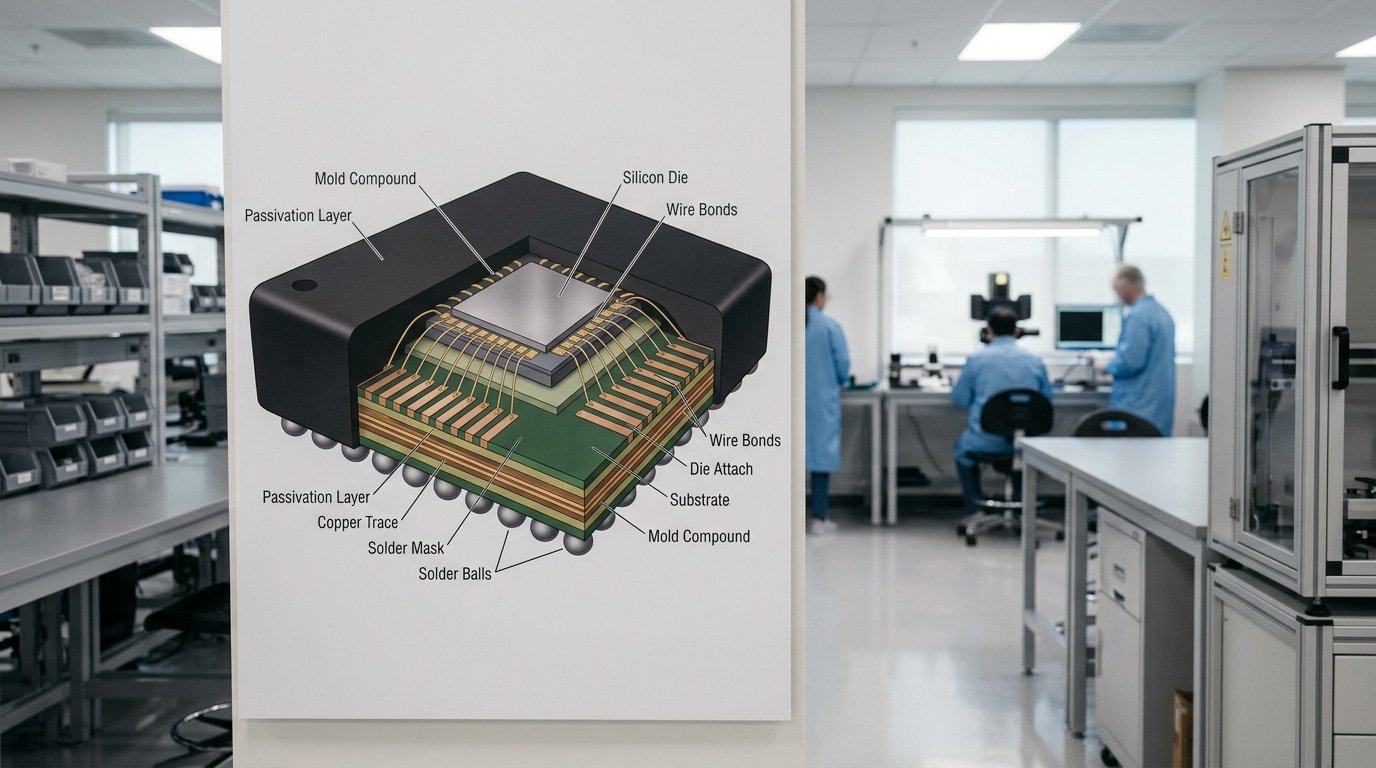
It bonds the tiny die to a substrate or leadframe, connects its electrical pads to the outside world, and seals it in a protective shell.
IC packaging is defined as the final fabrication stage where the die gets mechanical protection and electrical contacts. In short: it makes a chip you can actually solder onto a board.
Think of the bare die as a fragile glass sliver. It can’t survive humidity, handling, or heat on its own. Packaging gives it armor and wiring.
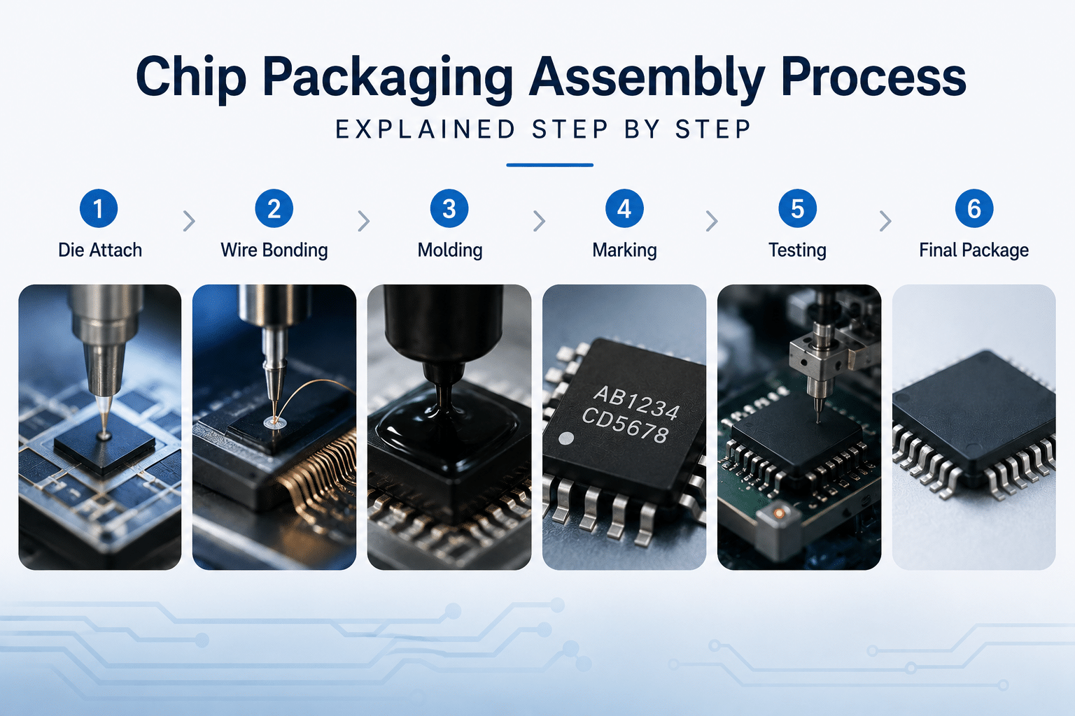
The full flow runs in a predictable order. A standard sequence covers wafer thinning, wafer dicing (cutting the wafer into chips), die attach, wire bonding or flip-chip interconnect, encapsulation, marking, solder ball attach or lead finish, trim-form-singulation, and final electrical testing.
Each step adds either a connection, a protection layer, or a quality gate.
Where does it sit? Right after Wafer fabrication (the front-end, where transistors are built) and right before Final test and shipping. The front-end builds the brain. Packaging builds the body that lets that brain talk to a phone, a server, or a car.
Why packaging now eats a bigger slice of chip cost
For decades, packaging was a cheap afterthought, a few percent of total cost. That math has flipped.
As transistors stopped shrinking cheaply, chipmakers turned to advanced packaging to keep gains coming. For leading-edge processors, packaging and test can now reach approximately 25% to 30% of total manufacturing cost, and for some multi-die designs it climbs higher.
Two forces drive this. First, fine-pitch interconnects and stacked dies demand expensive substrates and precision tools. Second, advanced methods like 2.5D and 3D integration put multiple chips into one package, which moves complexity from the wafer to the assembly floor.
- Mechanical protection — shields the die from shock, dust, and moisture
- Electrical connection — routes signals and power between die and circuit board
- Thermal path — moves heat away so the chip doesn’t cook itself
One practical tip engineers learn fast: design the package early, not last. A die laid out without a package plan often needs costly redesign when interconnect pitch or thermal limits don’t match.
Treat packaging as a co-design partner with the front-end, and you avoid the most expensive rework in the whole flow.
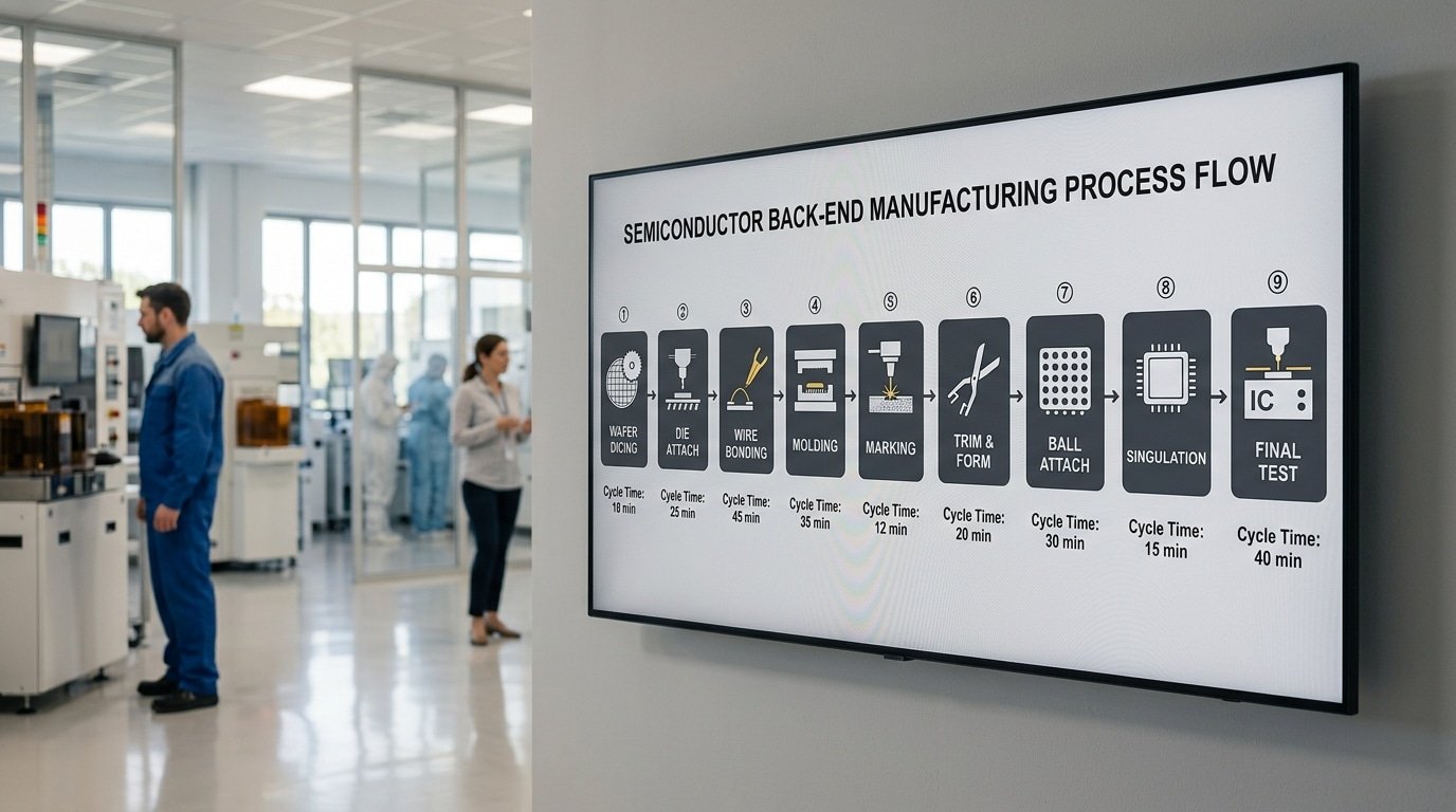
The Step by Step Assembly Flow From Wafer to Finished Package
A standard Chip packaging and assembly process moves through nine steps that happen one after another: thinning the wafer, dicing, die attach, interconnect, molding, marking, lead finish or solder ball attach, singulation, and the final test. Every stage passes along a half-finished unit to whatever comes next.
One little flaw early on can ruin the part hours later. By then, thousands of dollars in extra work have already been poured into it.
Here is the whole flow laid out, along with the gear and the rough timing you can expect on a line running lots of units:
| Step | Typical equipment | Cycle time per unit/batch |
|---|---|---|
| Wafer thinning + dicing | Backgrind tool, diamond saw or stealth laser | ~2–approximately 5 min per wafer to dice |
| Die attach | Pick-and-place bonder, epoxy dispenser | 0.1–0.5 s per die placement |
| Interconnect (wire bond) | Auto wire bonder (gold/copper wire) | 5–15 wires per second |
| Molding | Transfer molding press, EMC pellets | ~90–180 s cure per mold |
| Marking + plating | Laser marker, electroplating bath | ~1–3 s laser mark per part |
| Singulation | Saw or punch trim/form tool | Seconds per strip |
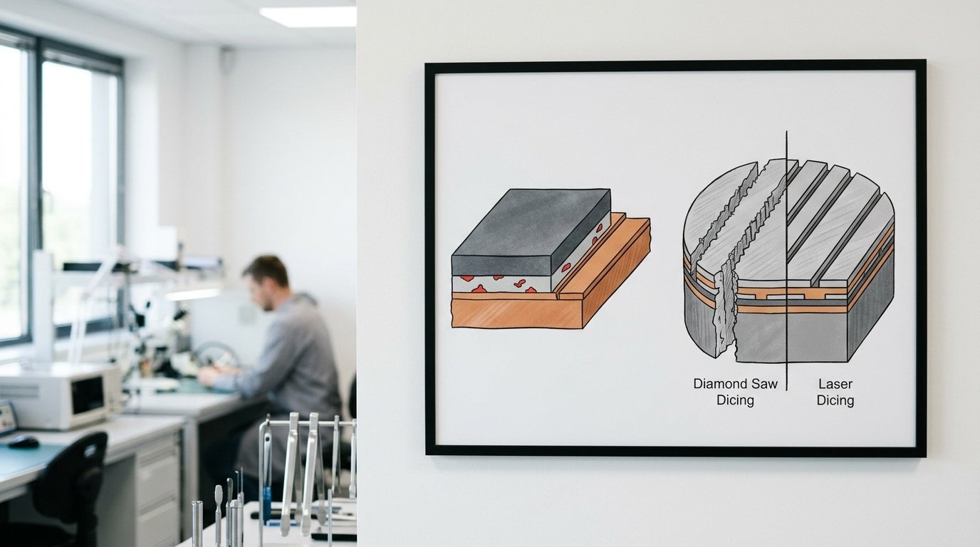
Dicing, which basically means cutting the wafer into separate chips, kicks off the back-end line. A diamond blade spins at over 30,000 RPM and leaves little streets just 30,80 microns wide between the dies.
Laser dicing makes narrower cuts and chips the brittle silicon less, so advanced logic chips are skipping the saw more and more.
Die attach bonds each chip onto a leadframe or substrate, using either epoxy or solder. This layer is really the main way heat escapes. Pick a bad adhesive, and you essentially trap the heat, which pushes the temperature up and shortens how long the device lasts.
Once the interconnect is done, Molding seals everything up. Heated epoxy molding compound flows around the wires and then hardens into that black shell you see on any chip. It keeps out moisture, shock, and corrosion.
The line wraps up with marking, where the part number gets lasered on top. Then comes the lead finish, a plating that makes soldering easier, and singulation.
That last step slices the molded strip into separate finished packages. Each unit then heads to a final electrical test before it gets shipped out.
Die Attach and Wafer Dicing — Where Hidden Yield Loss Begins
Most assembly yield loss starts here, before a single wire is bonded. Wafer dicing chips the die edges, and die attach traps voids under the bond line. Both defects often pass visual inspection but fail later under thermal stress.
Industry void-rate specs typically cap voiding under the die at 10,25 percent, depending on the application, automotive and power devices sit at the tight end.
Wafer dicing, also called wafer sawing, cuts the processed wafer into separate chips and is treated as the starting point of level-0 packaging in the chip packaging and assembly process, according to SK hynix’s process descriptions. You choose between a spinning diamond saw and a laser.
Saw dicing is cheaper and handles thick wafers well. But the blade puts mechanical force on the silicon, causing chipping along the cut line.
Chips that reach 30,50 microns deep can crack into active circuitry. Laser dicing (cutting with a focused beam instead of a blade) makes narrower streets and far less edge damage, which matters for thin or low-k dielectric wafers that crumble under blade pressure.
The tradeoff: laser tools cost more and run slower per wafer.
Why die-attach voids matter more than they look
Die attach bonds each die to a substrate or leadframe. It’s the first core assembly step and the primary heat path off the chip, as noted by AnySilicon’s assembly guide.
A void is an air pocket trapped in that bond layer. Air doesn’t conduct heat, so a 15 percent void pushes the hot spot temperature higher and shortens device life.
The bonding material drives both thermal performance and cost per die:
| Bond material | Thermal conductivity (W/m·K) | Relative cost | Best fit |
|---|---|---|---|
| Epoxy (silver-filled) | 3–60 | Lowest | Consumer logic, low-power ICs |
| Solder (e.g. SnAgCu) | 50–80 | Medium | Power and RF devices needing better heat flow |
| Sintered silver | 150–250 | Highest | SiC/GaN power, automotive, high-temp parts |
One practical tip: inspect every void rate with scanning acoustic microscopy (SAM), not optical tools, voids hide under the die where light can’t reach. For sintered silver, watch sintering pressure and temperature closely, since under-sintering leaves porosity that mimics voiding and quietly drops your thermal margin.
These die-attach and interconnect choices feed directly into the next decision: wire bond versus flip chip.
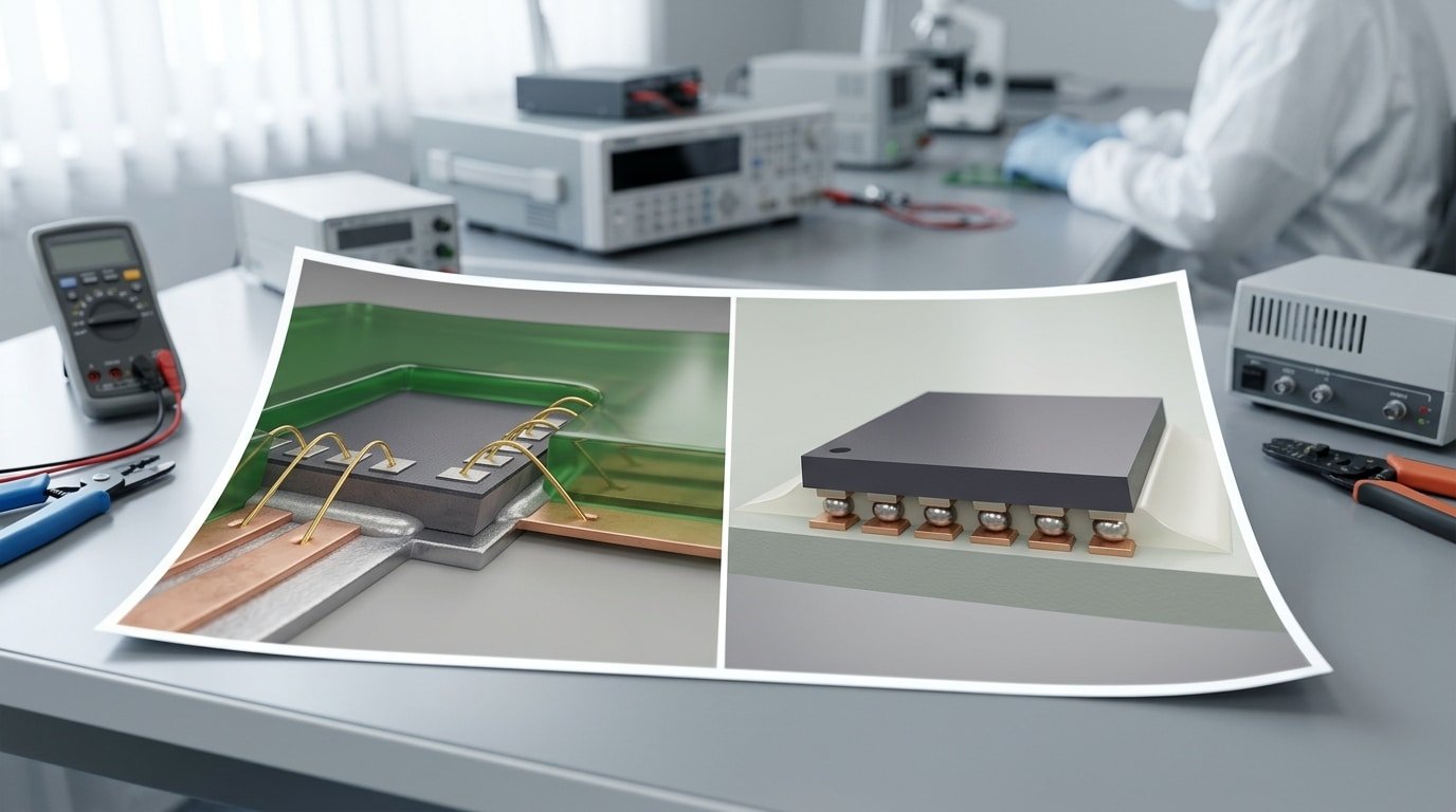
Wire Bond Versus Flip Chip — The Interconnect Decision That Drives Cost
Wire bonding tends to win on cost for chips with fewer than roughly 200 pins. Flip chip pulls ahead on speed and on how many connections you can pack in once pin counts push past 500.
The decision you make right here sets the lowest possible price for the entire chip packaging and assembly process. Why? Because the way you connect everything drives how complicated the base material gets, how long testing takes, and how much usable product comes out at the end.
Let me start with what each method actually does in physical terms. Wire bonding links the chip’s contact pads to the metal frame using very thin gold or aluminum wires, with one wire handling each connection.
Flip chip turns the chip face-down and joins it using tiny solder bumps, so every pad connects straight down into the base material below.
According to AnySilicon’s process guides, wire bonding is still the most commonly used connection method, while flip chip gives you shorter electrical paths and better electrical behavior overall.
The gold versus copper question matters here too. Copper wire really cut the cost of bonding material back when gold prices shot up. Though copper is a harder metal and needs much tighter control of bonding force, otherwise it can crater the soft aluminum pad sitting underneath.
A lot of assembly shops now run copper for high-volume consumer parts. They keep gold around for the delicate or low-volume chips.
| Interconnect | Relative cost (1x baseline) | Min pitch | Best for |
|---|---|---|---|
| Gold wire bond | 1.3x | ~40 µm | Low pin count, RF, legacy |
| Copper wire bond | 1.0x | ~35 µm | High-volume consumer ICs |
| Flip-chip bumping | 2.5x–4x | ~130 µm bump, scaling to micro-bump <40 µm | High I/O, high-speed, power |
Pitch is basically just the gap between one connection and the next. Wire bonding hits its limit around 35 to 40 µm because the wires need a little room so they don’t touch each other.
Flip chip spreads its bumps across the whole face of the chip. So a approximately 10 mm chip can carry thousands of connections, which wire bonding could never squeeze in along the edge alone.
The if-then rules:
- If your chip is under 5 mm with fewer than 200 pins, Use wire bonding. The flip-chip tooling and the underfill cost more than the part is really worth.
- If you need signal speed above a few GHz, or more than 500 connections, Use flip chip. Shorter paths cut down the inductance that wire loops tend to add.
- If you give off more than 5 W of heat, Lean flip chip. The bumps actually pull that heat down into the base material.
One practical trap I’ve seen. Flip chip needs underfill, which is an epoxy that fills the little gap under the chip.
Skip it and the heating and cooling cycles will crack the solder joints within months. That extra step eats into part of flip chip’s speed advantage on boards where cost matters a lot.
Molding, Underfill, and the Reliability Failures They Cause or Prevent
Molding seals the die in epoxy for protection; underfill fills the gap under flip-chip bumps to stop them cracking.
But both steps trap moisture and build mechanical stress, which is why popcorn cracking, delamination, and warpage almost always trace back here. Get the molding profile or moisture handling wrong, and a part that passed wire bond will fail months later in the field.
Transfer molding is the workhorse. Solid epoxy pellets are heated to about 175°C, liquefied, and forced under pressure into a mold cavity around the wire-bonded die.
The epoxy molding compound shields the chip from humidity, shock, and corrosion. The catch: that epoxy absorbs water from the air after molding.
Heat the part fast during board soldering, and trapped moisture flashes to steam.
That steam blows the package apart from inside. Engineers call it Popcorn cracking, the package literally pops like a kernel. It’s the single most common moisture failure in the chip packaging and assembly process.
MSL ratings: the moisture clock you can’t ignore
Moisture Sensitivity Level (MSL) tells you how long a package survives in open air before it must be soldered. The scale runs from MSL 1 (unlimited floor life) to MSL 6 (bake before every use).
Most modern thin BGAs land at MSL 3, giving you approximately 168 hours of exposure at approximately 30°C / approximately 60% relative humidity per JEDEC J-STD-020.
| MSL Level | Floor life (open air) | Practical handling |
|---|---|---|
| MSL 1 | Unlimited | No bake needed |
| MSL 3 | approximately 168 hours | Track time after bag opens |
| MSL 5 | approximately 48 hours | Bake if exposed too long |
| MSL 6 | Mandatory bake | 24h at approximately 125°C before reflow |
Practical tip: the moment a dry-pack bag opens, start the clock. Exceed floor life and you must bake the parts, typically approximately 24 hours at approximately 125°C, to drive moisture back out. Skip this on an MSL 3 part and field returns spike.
Underfill, warpage, and the height trade-off
Flip-chip parts need underfill, liquid epoxy drawn under the die by Capillary action (the same force that pulls water up a paper towel). It bonds the solder bumps to the substrate so thermal cycling doesn’t crack them.
Molded underfill (MUF) does the job in one molding shot for higher volume. Without it, bumps fatigue and open after a few thousand temperature cycles.
Thin packages bring a different enemy: Warpage. Silicon and epoxy shrink at different rates as they cool, so the package bows like a potato chip.
On a approximately 0.5 mm-thick fan-out package, warpage above 100 microns causes solder bridging or open joints at board assembly. Every micron of mold cap you add for protection adds package height, the core trade-off between durability and the thin profiles phone makers demand.
Delamination, the mold compound peeling from the die or leadframe, feeds all of these. Acoustic microscopy at incoming inspection catches it before it reaches your line.
Choosing a Package Type — A Decision Matrix for QFP, BGA, CSP, WLP, and 2.5D/3D
Pick by pin count first, then board space, then heat, then budget. Under 200 I/O with loose space limits?
⚠️ Common mistake: Skipping a controlled-atmosphere bake before die attach, which traps moisture and creates voids under the die. This happens because absorbed humidity flashes into vapor during the 150–approximately 300°C cure, leaving gaps that block heat flow and crack the die. The fix: bake substrates at approximately 125°C for 4+ hours and attach within the moisture-sensitivity window.
A QFP costs the least and ships fast. Above 300 I/O?
You need an area-array package like BGA or a flip-chip variant. Reach for 2.5D or 3D only when a single die physically can’t hold your function set, anything less is over-engineering you will pay for.
The trap most teams fall into: choosing the package by what looks modern instead of what the design needs. A wearable sensor with 48 pins doesn’t need wafer-level packaging.
A 5,000-pin AI accelerator can’t survive in a QFP. Match the family to the constraint that actually binds your design.
Decision factors that drive the choice
- I/O count — Sets the floor. Peripheral leads (QFP) max out near 300 pins before the package gets unwieldy. Area arrays scale to thousands.
- Board real estate — Chip-scale packages (CSP, where the package is within 1.2× the die size) and wafer-level packaging (WLP) win in phones and earbuds.
- Thermal load — Power above ~approximately 5 W usually demands a heat-spreader lid or a substrate with thermal vias, common in BGA and 2.5D builds.
- Budget — Each step up in pitch precision multiplies assembly cost.
| Package | Typical pitch | Cost tier | Best fit |
|---|---|---|---|
| QFP | 0.4–approximately 0.8 mm | Low | Microcontrollers, low-pin analog |
| BGA | 0.5–approximately 1.0 mm | Medium | FPGAs, application processors |
| CSP | 0.3–approximately 0.5 mm | Medium-high | Mobile DRAM, RF front-ends |
| WLP | 0.25–approximately 0.4 mm | High | Power management, image sensors |
| 2.5D/3D | <approximately 0.1 mm (microbumps) | Very high | HBM stacks, data-center GPUs |
When is advanced packaging justified? When you need bandwidth between dies that a printed circuit board can’t deliver.
Siemens engineering guides published in 2025 describe how 2.5D designs place dies on a silicon interposer with microbump pitches under 0.1 mm, roughly ten times finer than a standard BGA ball. That fine pitch is the whole point: it shortens die-to-die links and feeds memory-hungry processors.
But it also adds interposer fabrication, fine-pitch bonding, and harder thermal management to the chip packaging and assembly process, pushing unit cost well past conventional options.
Practical rule from the floor: if your design fits one die and stays under 300 pins, don’t even quote 2.5D. Validate a BGA first.
Move up only when simulation shows the board-level interconnect throttles performance. Skipping this check is how budgets blow out on parts that never needed an interposer.
Common Defects, Inspection, and Reliability Testing at the Assembly Stage
Five defects cause most assembly failures: bond lifting, voiding, solder bridging, delamination, and die cracks. Each needs a specific detection tool.
X-ray catches hidden voids and bridges, scanning acoustic microscopy (SAM) finds delamination, and 3D automated optical inspection (AOI) measures solder ball height. Qualification testing then proves the package survives field conditions before it ships.
Bond lifting means a wire pulls free from its pad. It often traces back to contaminated bond pads or wrong ultrasonic power.
Voiding is trapped air or gas inside solder or die-attach material. A void under the die blocks heat from escaping, raising junction temperature and shortening life.
Solder bridging is a short circuit where two adjacent balls or leads touch. Delamination is when molding compound separates from the die or leadframe, creating a gap that lets moisture in.
Detection tools map to specific defects. Here is how engineers match them:
| Defect | Best detection method | What it sees |
|---|---|---|
| Voiding in solder/die attach | 2D/3D X-ray (CT) | Air gaps under die or in BGA balls |
| Delamination | Scanning acoustic microscopy (SAM) | Separation at material interfaces |
| Solder bridging | X-ray + 3D AOI | Shorts between adjacent pads |
| Bond lifting | Wire pull and ball shear test | Weak or detached bonds |
| Die crack | SAM + cross-section | Fractures from dicing or molding stress |
SAM works by sending ultrasound through the package. When the wave hits a gap filled with air, it reflects back differently than solid material.
That reflection shows up as a bright spot on the scan. For voiding, JEDEC J-STD-020 sets the limit: most flip-chip underfill specs reject any single void larger than approximately 10% of the bump area.
Qualification tests screen different failure modes:
- Temperature cycling (TCT) — swings the part between -65°C and 150°C, often 1,000 cycles. It screens solder joint fatigue and delamination from mismatched expansion.
- HAST (Highly Accelerated carefully check) — runs at approximately 130°C and approximately 85% humidity under bias. It screens corrosion and moisture-driven shorts in a few days instead of months.
- MSL (Moisture Sensitivity Level) — rates how much humidity a package absorbs before reflow. A failed MSL part can pop during soldering, called the “popcorn effect.”
- Drop test — screens solder ball cracks in handheld devices, following JESD22-B111.
A practical tip: always run SAM both before and after temperature cycling. Delamination that passes at time zero often appears only after thermal stress. Skipping the post-stress scan is the most common gap in a weak chip packaging and assembly process audit.
Cost and Yield Impact Mapped Across the Full Assembly Flow
Across a standard chip packaging and assembly process, the interconnect step (wire bond or flip chip) and the package substrate together drive the largest share of unit cost, while die attach and dicing cause the most silent yield loss.
Push suppliers hardest on substrate sourcing and bump pitch, those line items move the bill of materials more than molding or marking ever will.
Here is the catch sourcing leads miss. A defect caught at incoming inspection costs pennies.
The same defect that escapes to final test costs the full die value plus all assembly labor sunk into it. Cost compounds downstream, that’s the rule that should shape where you spend audit time.
| Assembly step | Relative cost share | Typical yield-loss point | Where to push the supplier |
|---|---|---|---|
| Wafer thinning + dicing | Low | Edge chipping, microcracks | Blade vs. laser spec, kerf width |
| Die attach | Low–medium | Voiding under die, delamination | Void % limit in X-ray spec |
| Interconnect (wire/flip chip) | High | Bond lift, bridging, open bumps | Bond pull data, bump pitch capability |
| Substrate / leadframe | High (advanced packages) | Warpage, plating defects | Second-source qualification, warpage limit |
| Molding + underfill | Medium | Voids, popcorn cracking | MSL rating, cure profile records |
| Final test + burn-in | Medium–high | Escapes, test coverage gaps | Test coverage %, ATE recipe access |
For advanced packages, the substrate flips the cost picture entirely. In conventional QFP, the leadframe is cheap.
In 2.5D builds, the silicon interposer and fine-pitch substrate can exceed the die cost itself, because 2.5D and 3D integration relies on advanced substrates and dense interconnects that few vendors can produce at yield.
Run the cost-of-escape math before you negotiate. A die worth approximately $40 at die attach carries roughly $8,$12 of added assembly value by final test.
Scrap it after molding and you lose the full stacked cost, not just the silicon. This is why a approximately 1% void escape at die attach hurts far more than a approximately 1% reject caught at incoming wafer inspection.
Practical rule for sourcing: demand statistical process control data on the two compounding steps, interconnect and substrate. Ask for bond pull histograms and warpage trend charts, not pass/fail summaries. Suppliers who hide trend data are usually hiding drift.
How Packaging Is Shifting From Conventional to Advanced 2.5D and 3D Integration
Advanced packaging splits one big chip into several smaller “chiplets” and reconnects them inside the package. This replaces the old habit of cramming every function onto one giant die. Why the change?
Big monolithic dies yield poorly and cost too much, so engineers now bond multiple small dies side by side (2.5D) or stacked vertically (3D) to hit the same performance for less money.
A chiplet is just a small, function-specific die, say, one for compute, one for memory, one for I/O. Each is built on the process node that suits it best.
The compute chiplet might use a leading-edge node; the I/O chiplet can use an older, cheaper one. That mix-and-match approach is called heterogeneous integration, and it sits at the heart of modern Chip packaging and assembly process design.
Three core technologies make it work:
- Silicon interposers — a thin silicon slab that carries dense wiring between chiplets in 2.5D layouts. Think of it as a tiny circuit board made of silicon.
- TSVs (through-silicon vias) — vertical copper tunnels drilled straight through a die so signals pass top-to-bottom in stacked 3D chips.
- Hybrid bonding — directly fusing copper pads on two dies with no solder bumps, reaching pitches under 10 micrometers versus 40+ for older bumps.
Fan-out wafer-level packaging (FOWLP) is the budget option. It spreads connections across an area larger than the die using a molded reconfigured wafer, skipping the substrate.
Apple’s A-series mobile processors have used TSMC’s InFO fan-out line since 2016, and the method now ships in hundreds of millions of units yearly.
The cost reality is sharp. Advanced packaging is the fastest-growing slice of the supply chain, Yole Group projects the advanced packaging market to reach roughly $78 billion by 2028, far outpacing conventional packaging.
But 2.5D builds carry a premium: a silicon interposer can add tens of dollars per unit, and hybrid bonding demands sub-100-nanometer alignment that few fabs can run at volume.
Assembly complexity climbs accordingly. As Siemens engineering guides published in 2025 describe, stacked configurations need advanced substrates, fine-pitch interconnects, and heat-removal strategies that conventional flows never faced.
Practical tip: thermal density is the real bottleneck, stacking logic on logic traps heat, so most 3D designs put memory on top and compute on the bottom, where the heat spreader can reach it.
Frequently Asked Questions About Chip Packaging and Assembly
Quick answer: Packaging refers to the protective case and electrical connections built around the die. Assembly refers to the physical steps that build that case, die attach, bonding, molding, and singulation. Most engineers use the two words together because you can’t have one without the other.
What’s the difference between packaging and assembly?
Packaging is the noun. Assembly is the verb. The IC packaging definition on Wikipedia describes packaging as the final fabrication stage where the silicon die gets a protective case plus electrical contacts to the outside world.
Assembly is how you get there. When a vendor quotes you a “chip packaging and assembly process,” the packaging part names the end product (a BGA, a QFP, a flip-chip module), and the assembly part lists the line steps needed to make it.
Treat them as one quote, not two.
Why does flip chip cost more than wire bond?
Flip chip needs solder bumps deposited on every die pad, plus underfill, plus a finer substrate. Wire bond just needs a leadframe and a bonder. The bumping step alone adds a full wafer-level process before assembly even starts.
For a chip under 200 pins, that extra tooling rarely pays off. Flip chip wins only when pin count, signal speed, or heat demands shorter interconnects, think GPUs and server CPUs, not a power management IC.
What causes package delamination?
Delamination is when layers inside the package peel apart, usually the mold compound lifting off the die or substrate. Three culprits dominate:
- Moisture trapped before molding. Water turns to steam during reflow and pops layers apart (the “popcorn effect”). This is why parts ship in dry packs with a humidity indicator card.
- Mismatched thermal expansion. Mold compound and silicon expand at different rates when heated, creating shear stress at the interface.
- Contaminated die surface. Even fingerprint-level residue weakens the epoxy bond.
Scanning acoustic microscopy (a tool that uses sound waves to see inside the package) catches delamination before it ships.
How do you read a packaging process flow chart?
Read left to right, top to bottom, and treat each box as a yield gate. A standard flow runs wafer thinning, dicing, die attach, bonding, molding, marking, ball attach or lead finish, singulation, then final test. Diamond shapes mark inspection or test decision points where parts can be rejected.
The trick is reading what’s Not drawn. Look for moisture-bake steps before molding and underfill steps after flip-chip attach, flows that skip these on the diagram often skip them on the line too.
Key Takeaways for Engineers and Sourcing Leads
Treat the Chip packaging and assembly process as a chain of trade-offs, not a fixed recipe. Every step you save on cost moves risk somewhere else: a cheaper interconnect raises thermal limits, a smaller package raises board-level stress, a faster cure time raises void rates.
Your job is to decide where you can afford that risk for your specific product.
Start with the part the prior sections proved costs you the most. Interconnect choice and yield loss at dicing drive the biggest swings. Get those two locked before you argue about lid attach or marking.
A Vendor and Process Checklist Before You Sign
- Interconnect fit: Confirm wire bond below ~200 pins, flip chip above. Ask for the vendor’s own yield data at your pin count, not a generic average.
- Dicing method: For dies under 100 µm thick or low-k dielectric layers, demand laser or plasma dicing. Blade sawing on these materials chips edges and quietly bleeds yield.
- Underfill spec: For flip chip, get the capillary underfill cure profile in writing. Voids here cause field failures that test never catches.
- Reliability evidence: Require JEDEC moisture sensitivity level (MSL) data and temperature cycling results. A vendor without these is asking you to be their test lab.
- Thermal path: For parts above approximately 5 W, ask whether they add a metal lid with thermal interface material and what junction temperature that buys you.
Map your product against the decision matrix from the package-selection section. A microcontroller for a thermostat and a data-center accelerator share zero packaging answers. Pin count, board space, heat, and budget rank in that order for most designs.
One reality check on the advanced path. The 2.5D and 3D route using interposers and stacked dies, described in 2025 Siemens engineering guides, delivers real bandwidth gains but adds fine-pitch interconnect and thermal complexity that small-volume products rarely justify.
If your shipment count is under a few hundred thousand units a year, conventional BGA or QFP almost always wins on total cost.
Run your own bill of materials through this lens before the first request for quote. Write down your pin count, power budget, target board area, and unit volume.
Those four numbers decide most of the Packaging and assembly path for you. Bring them to the vendor instead of asking the vendor to pick.
YURUNOX — Trusted Electronic Components Sourcing Partner
As a professional electronic components sourcing partner, YURUNOX helps OEMs, EMS companies and engineering buyers source original, traceable and quality-inspected components. Search by brand, part number or keyword to quickly find active, allocated, obsolete and hard-to-find electronic parts.
- ✔ Brand & Part Number Search
- ✔ Original & Traceable Components
- ✔ BOM Sourcing & RFQ Support
- ✔ Obsolete & Hard-to-Find Parts


