Chip wafer manufacturing equipment turns raw silicon wafers into finished chips like integrated circuits, and the six main process families are lithography, etch, deposition, implant, metrology, and thermal processing (Wafer fabrication equipment, 2026).
Each family handles one step in building the tiny transistor layers stacked on a single wafer.
This guide breaks down what each tool type does, where it fits in the fab line, and which use cases drive demand in 2025,2026, from EUV scanners that print sub-7nm features to atomic-layer deposition systems that lay down films just a few atoms thick.
Quick Takeaways
- EUV lithography is essential for sub-7nm nodes but remains supply-constrained, limiting fab throughput.
- Six front-end tool families: lithography, deposition, etch, implant, CMP, and metrology.
- Advanced chips need 1,000+ process steps, cycling tools repeatedly to stack 15+ layers.
- Each tool class controls one specific defect, from overlay misalignment to surface unevenness.
- Metrology adds no features but catches escaped defects and process drift early.
How Wafer Manufacturing Equipment Maps to the Process Flow
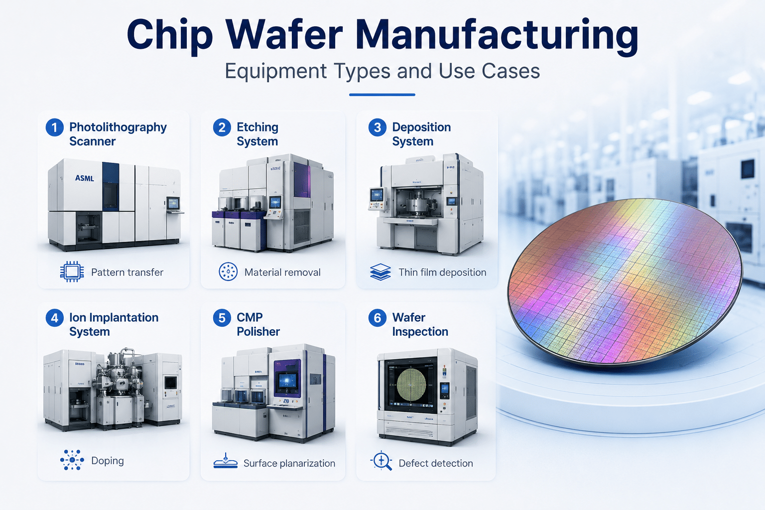
Chip wafer manufacturing equipment falls into two halves: front-end tools that build circuits onto a bare silicon wafer, and back-end tools that thin, cut, and package those wafers into finished chips. Six core front-end tool classes do the heavy lifting, lithography, deposition, etch, ion implant, chemical mechanical planarization (CMP), and metrology, and each one owns a specific defect it must prevent.
The sequence repeats in loops. A single advanced chip can require Over 1,000 process steps and cycle through the same tool classes dozens of times to stack 15+ layers. Here is what each tool does and the failure it controls:
| Tool class | Process step | Defect it controls |
|---|---|---|
| Lithography | Prints circuit pattern into photoresist | Overlay misalignment, blurred edges |
| Deposition (CVD/PVD) | Grows thin film layers | Thickness variation, voids |
| Etch | Removes material to carve features | Undercut, sidewall roughness |
| Ion implant | Dopes silicon to set conductivity | Wrong dose, channeling |
| CMP | Flattens each layer before the next | Dishing, surface unevenness |
| Metrology | Measures and inspects after key steps | Escaped defects, drift |
Lithography sets the pace. EUV lithography is indispensable for nodes below 7nm and stays supply-constrained, making it the bottleneck that decides how fast a fab can run.
One pro insight: metrology never adds a feature, yet skipping it’s how a approximately $20,000 wafer lot becomes scrap. Inspect after etch and CMP, where overlay and surface errors compound into the next layer, not just at final test.
This map is the spine of every wafer fabrication equipment decision that follows.
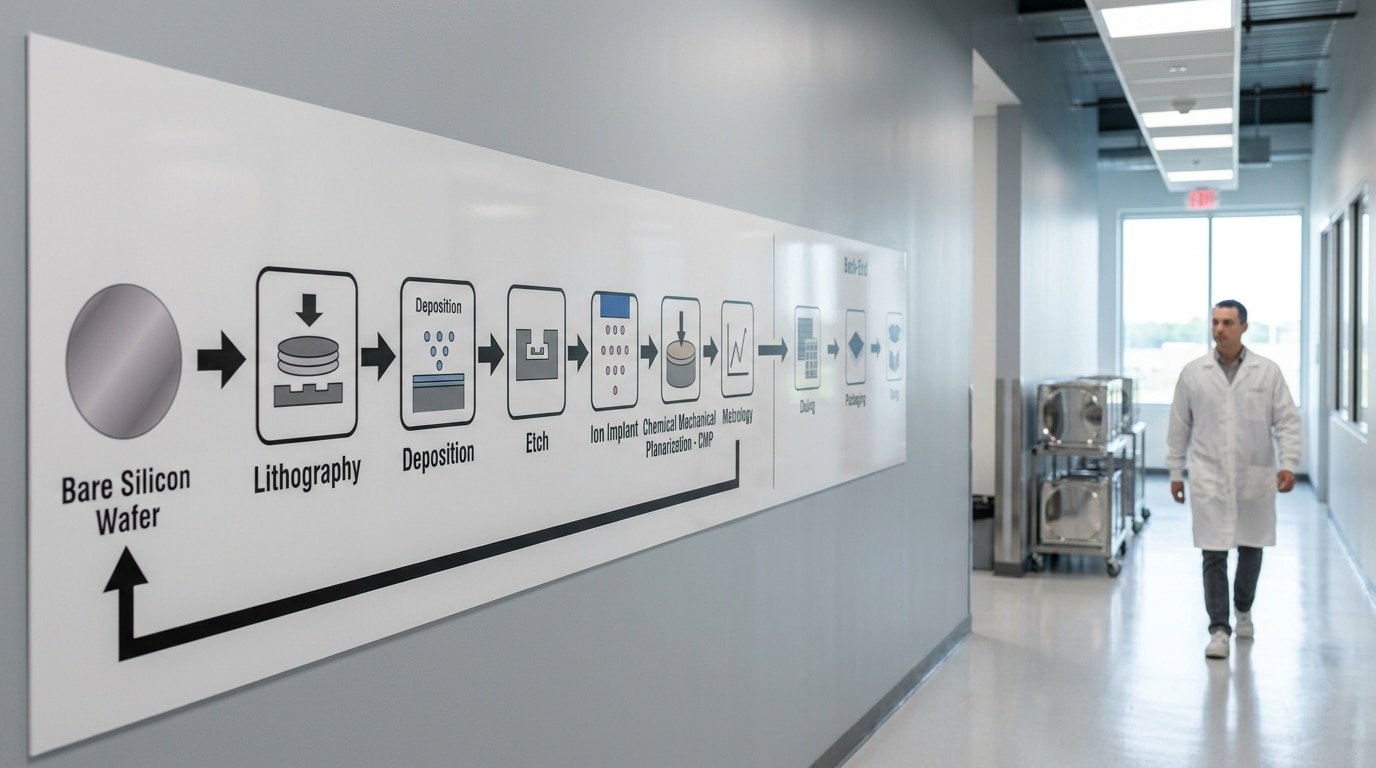
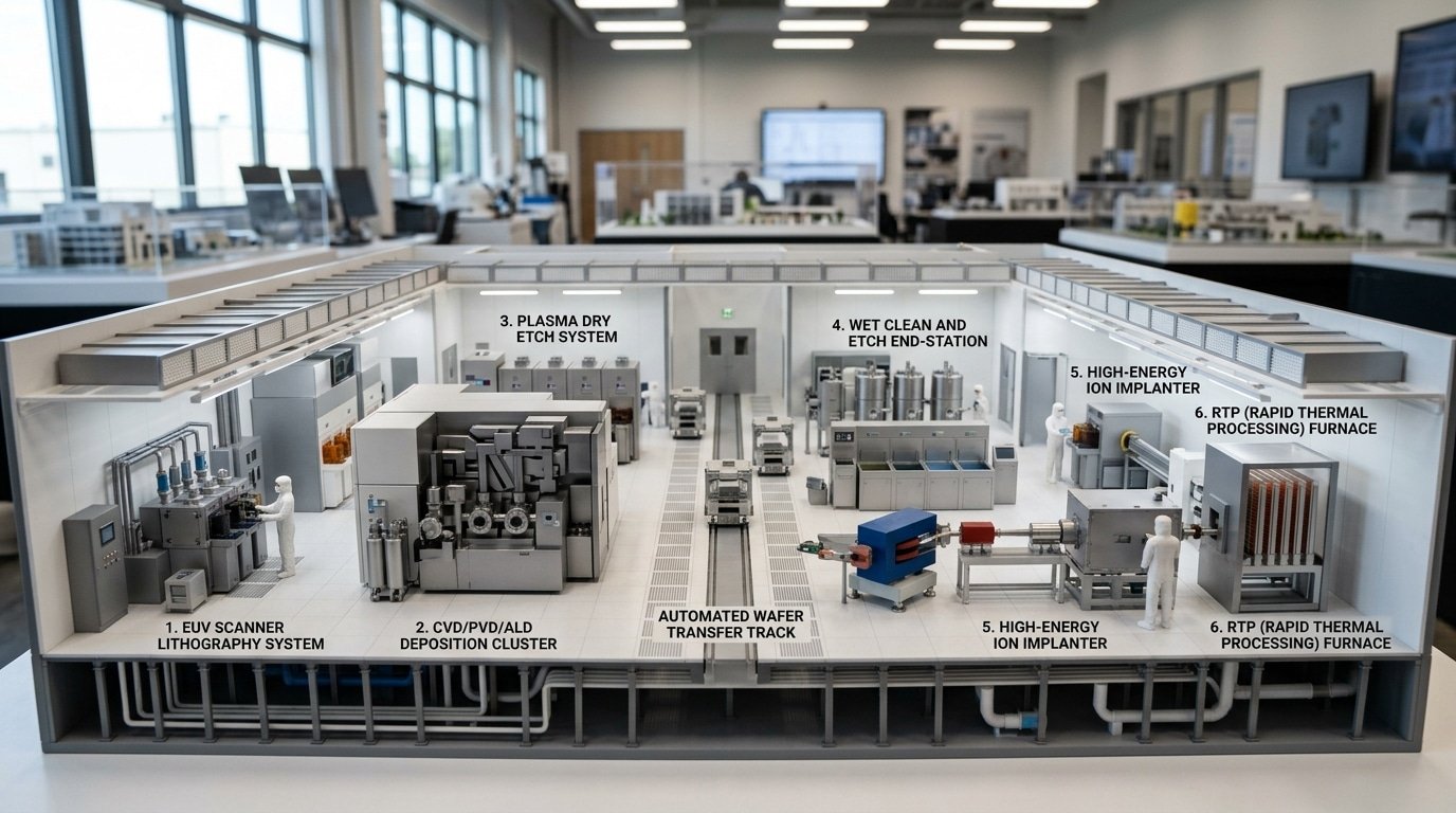
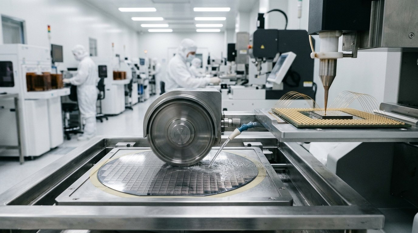
Front-End Equipment Types and What Each One Does
So there are basically six families of tools that do most of the real work inside a wafer fab. You’ve got lithography scanners, deposition reactors (which include CVD, PVD, and ALD), etchers, ion implanters, and thermal processors.
These categories essentially build the transistors and the wiring that turn a blank silicon disc into a working chip.
They also eat up the biggest chunk of money being spent. The global market for this kind of gear is projected to grow from USD 166.35 billion in 2025 to USD 344.36 billion by 2032.
Lithography scanners and steppers print the circuit patterns onto a light-sensitive coating, the stuff they call photoresist. Extreme ultraviolet tools, or EUV, are indispensable for chip nodes below 7nm, and honestly they’re still really hard to get worldwide.
A single EUV system can run past approximately $200 million, which is exactly why fabs obsess over keeping their scanners running.
Deposition tools grow the thin films. CVD, meaning chemical vapor deposition, uses gas reactions to lay down insulating layers. PVD sputters metal for the wiring. And ALD, the atomic layer one, builds films a single atomic layer at a time, which makes the thinnest gate insulators you can get.
Etchers carve out the patterns. The plasma kind, which is dry, uses ionized gas for precise vertical cuts. Wet etchers, on the other hand, use chemical baths for cleaning and stripping away bulk material.
Ion implanters fire dopant atoms into the silicon to set how it behaves electrically. RTP (rapid thermal processing) furnaces heat the wafers to over 1,000°C in just seconds, which activates those dopants without letting them drift out of place.
Put together, these chip wafer manufacturing equipment classes really create every active layer sitting below the metal stack.
CMP, Cleaning, and Metrology Tools That Control Yield
These three tool classes don’t build the chip, they decide whether it survives. CMP flattens each layer, cleaners strip contamination between steps, and metrology systems measure whether the pattern landed where it should. Skip the investment here and your fancy lithography output still scraps at the test floor.
Chemical mechanical planarization (CMP) grinds and polishes a wafer flat after each deposition layer. Picture a spinning pad pressing the wafer against a slurry of tiny abrasive particles.
A wafer can pass through CMP 15 to 20 times across a full process flow. If the surface isn’t flat to within a few nanometers, the next lithography step can’t focus, the depth of field on a deep-ultraviolet scanner is that tight.
Cleaners come in two builds. Batch cleaners dunk 25 to 50 wafers at once for throughput. Single-wafer cleaners handle one wafer at a time for tighter control on advanced nodes. RENA Technologies supplies batch, single-wafer, and spray wet-processing systems for exactly this split.
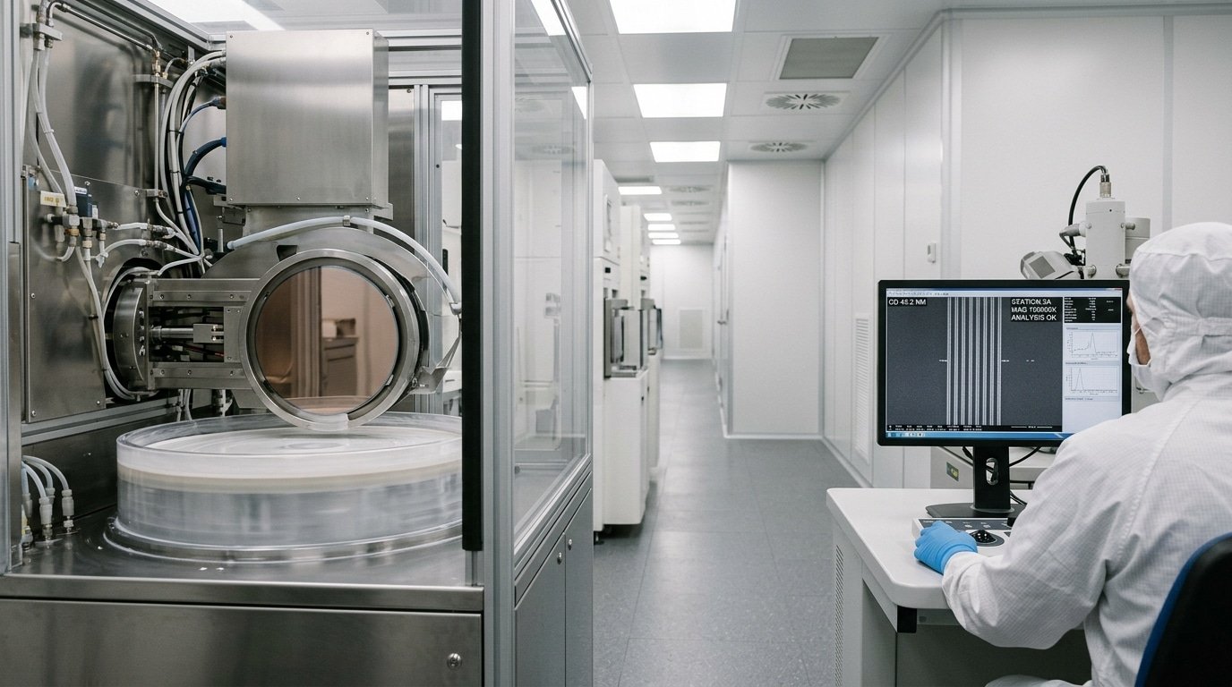
Metrology is the camera that never blinks. Overlay tools confirm each new layer aligns with the one below.
CD-SEM (critical dimension scanning electron microscopy) measures feature width down to the nanometer, a transistor gate that’s 3nm wide must measure 3nm, not 3.4nm, or the transistor’s switching speed and leakage drift out of spec.
A single misaligned overlay measurement caught early can save thousands of wafers from running defective.
This support equipment is the quiet half of Chip wafer manufacturing equipment spending. The broader market is projected to reach USD 344.36 billion by 2032, and metrology’s share grows fastest as nodes shrink and each new layer demands tighter measurement.
Back-End Handling, Wafer Thinning, Dicing, and Packaging Equipment
Once the wafer leaves the fab with all its circuits printed onto it, a completely different set of machines takes over. These are assembly and packaging tools. They aren’t the same as the Chip wafer manufacturing equipment used in the front-end part of the process.
The industry sorts this gear into three groups. There’s wafer fabrication, then assembly and packaging, and finally test, the way WaferWorld lays it out. Honestly, buyers mix these up constantly.
Here is the simple rule though. Front-end tools build the circuit on the wafer itself. Back-end tools cut that wafer apart and turn each piece into a chip you can actually use. They sit in rooms that are cleaner but cheaper, and they cost far less per unit.
The core back-end tools, in order of use
- Backgrinders — These thin the wafer down from around 775 microns to somewhere between 50 and 100 microns. Thin chips are what fit into phones and stacked memory. Push it too far and the wafer just cracks.
- Dicing saws — These cut the wafer into individual dies, which are the separate chip pieces. They use either a blade spinning at 30,000 RPM or a laser. Laser dicing leaves cleaner edges on brittle low-k chips.
- Die attach machines — These glue or solder each die onto a lead frame or a substrate, which is basically the base it sits on.
- Wire bonders — These connect the chip’s contact pads to the package pins. They use gold or copper wires that are thinner than a human hair, around 18 to 25 microns.
Advanced packaging tools take things even further. You’ve got flip-chip bonders, through-silicon via drills, which are tools that drill tiny vertical holes called TSVs, plus 2.5D interposer machines.
These drive growth now, since stacking chips on top of each other works better than shrinking them at the hardest nodes. Edge grinders from vendors like Daitron smooth the wafer rims before thinning, which stops the edges from chipping.
One practical tip from my experience. Always match the dicing tape thickness to the die size. The wrong tape causes die flyaway, and you end up losing good chips after they survived the entire fab.
Equipment Cost Tiers by Tool Class with Real Price Ranges
The single most expensive tool in a fab is an EUV lithography scanner, which runs above approximately $150 million per unit.
From there, prices drop sharply by tool class, etch and deposition systems land in the approximately $5,20 million range, while entry-level diffusion or wet-bench tools can cost under $1 million.
Lithography alone often eats 30,40% of a leading-edge fab’s tool budget.
EUV (extreme ultraviolet light, used to print features below 7nm) sits in a tier of its own. These scanners are globally supply-constrained and indispensable for advanced nodes, which is why a single delivery slip can push a fab’s schedule back by a year.
| Tool Class | Price Per Tool (USD) | Budget Role |
|---|---|---|
| EUV scanner | approximately $150M+ | Single largest line item; pacing item for <7nm |
| DUV immersion scanner | approximately $50M–$80M | Workhorse for mature and mid-range nodes |
| Ion implanter (high current) | approximately $10M–$25M | Doping; multiple units per fab |
| Etch / CVD / PVD system | approximately $5M–$20M | Bought in clusters; high tool count |
| CMP polisher | approximately $3M–$8M | Yield control; scales with metal layers |
| Entry wet-bench / diffusion | approximately $0.3M–$1M | Low-cost, high-volume support tools |
Here is what budget planners miss: tool count multiplies cheap tools into big numbers. A fab may run 40 etch chambers but only 5 EUV scanners, so a approximately $10M etch tool class can rival lithography in total spend.
The global chip wafer manufacturing equipment market reflects this scale, projected by MarketsandMarkets to reach approximately $344.36 billion by 2032.
How Much It Costs to Fabricate a Wafer End to End
A finished approximately 300mm wafer costs roughly $1,500,$3,000 at a mature node and $13,000,$20,000 at a leading-edge node like 3nm or 5nm. Equipment depreciation alone accounts for 60,approximately 70% of that cost, more than materials, labor, and energy combined.
Why does the gear dominate? A single fab packs billions of dollars of chip wafer manufacturing equipment, and accountants write that hardware off over about five years.
Spread that depreciation across the wafers the fab produces, and each wafer carries a heavy fixed charge before any silicon is even touched.
Here is how the per-wafer dollars typically split at a leading-edge node:
- Equipment depreciation: 60–approximately 70% — the largest single line item
- Materials and replacement parts: 10–approximately 15% — photoresist, specialty gases, CMP slurry, target metals
- Direct labor: 5–approximately 8% — fabs run lights-out, so headcount per wafer is low
- Facilities and energy: 8–approximately 12% — cleanroom air, ultrapure water, power
Yield loss multiplies all of it. If 80 of 100 dies pass, every cost above gets divided by fewer good chips. A 10-point yield drop at a 5nm node can add hundreds of dollars per usable wafer of output.
Mature nodes flip the math. Older tools are often fully depreciated, so a 28nm wafer leans more on materials and labor.
That’s why a paid-off approximately 200mm line can stay profitable for decades. The pressure on equipment ties back to a market projected to reach USD 344.36 billion by 2032.
Leading Equipment Vendors and Their Typical Fab Use Cases
Five companies dominate chip wafer manufacturing equipment, and each owns a different step. ASML alone makes EUV lithography scanners.
Applied Materials leads deposition and ion implant. Tokyo Electron and Lam Research split etch and coat/develop.
KLA owns inspection and metrology. Knowing who supplies what tells you where your lead times and bottlenecks will come from.
ASML has a monopoly on extreme ultraviolet (EUV) machines, the only tools that can print features below 7nm. No competitor sells one.
That single fact constrains every leading-edge fab. The broader equipment market is growing fast too, projected to climb from USD 166.35 billion in 2025 to USD 344.36 billion by 2032, an approximately 11% annual rate.
| Vendor | Leads in | Typical use case |
|---|---|---|
| ASML | EUV + DUV lithography | Patterning sub-7nm logic and advanced DRAM |
| Applied Materials | CVD, PVD, ion implant, CMP | Layer deposition and doping across all nodes |
| Lam Research | Plasma etch, deposition | 3D NAND stacks and high-aspect-ratio etch |
| Tokyo Electron | Coat/develop, etch, clean | Photoresist tracks paired with ASML scanners |
| KLA | Inspection, metrology | Defect detection and overlay measurement |
Practical tip: pair vendors by interface. TEL coat/develop tracks dock directly to ASML scanners on the same lithography cell, so most leading fabs buy them together.
Applied Materials states its tools deposit layers, shape materials with atomic precision, and analyze devices, which is why it shows up at more process steps than any other supplier.
Used, Refurbished, and Entry-Level Equipment for Labs and Startups
You don’t need a new approximately $50 million tool to run a research fab. A refurbished deposition or etch system from a vendor like Applied Materials or Lam Research typically sells for 30,approximately 70% below new list price, and many ship with a 90-day warranty plus installation support.
For university labs and startups working at mature nodes, this is the only realistic path into Chip wafer manufacturing equipment.
The secondary market splits into three tiers. Knowing the difference saves you from costly mistakes.
| Tier | Price vs. new | What you give up |
|---|---|---|
| As-is / parts | 5–approximately 20% | No warranty, no install, often non-working |
| Refurbished (vendor) | 30–approximately 60% | Older node capability, limited spares |
| Refurbished (3rd party) | 20–approximately 45% | No OEM support, software license gaps |
The hidden trap is node capability. A used approximately 200mm tool built for the 130nm process can’t suddenly run 28nm, the optics, stage precision, and control software cap it. Most lab buyers want approximately 150mm or approximately 200mm wafers anyway, where mature equipment is plentiful and cheap.
Watch the support cliff. OEMs stop selling spare parts for tools roughly 10,15 years after launch. Once that happens, a single failed turbomolecular pump can idle your tool for months. Always confirm parts availability before buying.
The broader market keeps used tools flowing. MarketsandMarkets projects equipment sales to hit approximately $344.36 billion by 2032, and every fab upgrade dumps older tools into the resale channel. Buy where the supply is fat.
Frequently Asked Questions
Quick answers to the questions buyers ask most before they commit to a tool or a fab plan.
How much does it cost to fabricate one wafer?
A finished approximately 300mm wafer runs about $1,500,$3,000 at a mature node and $13,000,$20,000 at a leading-edge node like 3nm. The gap comes from mask layers: leading-edge designs need over 80 photomask layers, each adding lithography, etch, and metrology passes.
What does “wafer fab equipment” actually mean?
Wafer fab equipment (WFE) means the machines that turn a blank silicon wafer into a wafer full of finished circuits. Per Wikipedia’s WFE entry, the main families are lithography, etch, deposition, implant, metrology, and thermal processing.
It usually excludes assembly and test gear, which sit in the back-end category.
Which companies supply chip manufacturing machines?
ASML builds lithography scanners. Applied Materials and Lam Research cover deposition and etch. Tokyo Electron spans coat/develop and etch, and KLA owns inspection and metrology. For wet processing, RENA Technologies supplies batch and single-wafer etching tools.
Where can you find chip wafer manufacturing equipment for sale?
New tools come direct from vendors with 12,18 month lead times. For used and refurbished units, check SurplusGlobal, EquipNet, and Daitron. Always demand a pre-shipment process qualification run, a “working” tool that misses spec by 2nm is scrap for a real fab.
Building Your Equipment Selection Sequence
Start with your node target, then work backward to tools. A mature 65nm or 28nm line lets you skip EUV entirely and lean on used i-line or deep-UV scanners.
A line below 7nm forces you into EUV lithography, which is globally supply-constrained and described as indispensable for those nodes. Your node decides approximately 60% of your tool list before you call a single vendor.
Use this sequence to turn budget and yield goals into a real shopping order:
- Lock your node and wafer size. approximately 200mm versus approximately 300mm changes every tool’s handling spec and price.
- Set a yield floor. Want approximately 90%+ at a fine pitch? Budget for inline metrology and advanced CMP, not just the patterning tools.
- Buy the bottleneck first. Lithography and etch carry the longest lead times — order these before deposition or cleaning.
- Match capital to volume. A research lab running 50 wafers a month should weigh refurbished single-wafer tools over new batch systems.
One practical trap: people buy a scanner and forget the resist track and metrology that feed it. A lithography cell is three tools, not one. Skip the metrology and your yield data stays blind.
The market reflects how fast these decisions are getting harder. MarketsandMarkets projects chip wafer manufacturing equipment spending to rise from USD 166.35 billion in 2025 to USD 344.36 billion by 2032, an approximately 11.0% CAGR, meaning lead times and prices climb yearly.
Your next step: list your tools by process family, then request quotes by category, lithography, etch, deposition, CMP, metrology, and back-end dicing. Match each quote against the cost tiers and vendor use cases covered earlier in this guide.
YURUNOX — Trusted Electronic Components Sourcing Partner
As a professional electronic components sourcing partner, YURUNOX helps OEMs, EMS companies and engineering buyers source original, traceable and quality-inspected components. Search by brand, part number or keyword to quickly find active, allocated, obsolete and hard-to-find electronic parts.
- ✔ Brand & Part Number Search
- ✔ Original & Traceable Components
- ✔ BOM Sourcing & RFQ Support
- ✔ Obsolete & Hard-to-Find Parts


