This comparison of DRAM, SRAM, NAND, and NOR comes down to one rule: choose SRAM for fastest on-chip cache, DRAM for large working memory, NAND for bulk storage, and NOR for boot code run directly from the chip. In 2023, SRAM’s 6-transistor (6T) cell ran 3.6× larger in area than DRAM’s 1T1C cell at the same node (Infineon). SRAM and DRAM lose data instantly when power drops, while NAND and NOR retain data for 5–10 years.
That single physical difference drives almost every trade-off you face when choosing memory.
This comparison of DRAM, SRAM, NAND, NOR breaks down which one fits your design: pick SRAM for raw speed and zero latency, DRAM for cheap high-density working memory, NAND for bulk storage, and NOR for code you run directly from the chip.
Quick Takeaways
- Choose SRAM for cache, DRAM for working memory, NAND for storage, NOR for boot code.
- SRAM and DRAM lose data instantly; NAND and NOR retain it 5–10 years.
- Use SLC NAND (50,000+ cycles) over TLC NAND (3,000–5,000) for endurance-critical writes.
- Expect SRAM’s 6T cell to need 3.6× more area than DRAM.
- Pick NOR for execute-in-place boot code; pick NAND for bulk storage density.
DRAM vs SRAM vs NAND vs NOR at a Glance
Quick answer: Pick SRAM for the fastest on-chip cache, DRAM for large working memory, NAND for bulk storage, and NOR for boot code you run directly. SRAM and DRAM lose data the instant power drops.
NAND and NOR keep it for years. The table below settles approximately 90%[1] of selection questions in 30 seconds.
| Property | SRAM | DRAM | NAND | NOR |
|---|---|---|---|---|
| Volatility | Volatile | Volatile | Non-volatile (5–10 yr retention) | Non-volatile (5–10 yr retention) |
| Relative cost-per-bit | Highest | Moderate | Lowest | High (low density) |
| Endurance (write cycles) | Practically unlimited | Practically unlimited | 3,000–100,000 P/E | ~100,000+ P/E |
| Access granularity | Byte / word | Byte / word (row-based) | Page read, block erase | Byte read, block erase |
| Primary use case | CPU L1/L2/L3 cache | System main memory | SSDs, phone storage | Boot ROM, firmware |
Why does volatility split the four into two camps? In 2024, DRAM stayed volatile, losing data within milliseconds of power loss, while NAND and NOR held data for 5,10 years at room temperature. That single trait decides whether you store running calculations or saved files.
Endurance separates the flash pair too. SLC NAND survives 50,000,100,000 program/erase cycles; cheaper TLC NAND drops to roughly 3,000,5,000. NOR sits at the high end but stores far fewer bits per chip, which is why engineers reach for it to hold boot code rather than user data.
This Comparison of DRAM, SRAM, NAND, NOR sets the frame. The sections ahead unpack each cell structure, real latency numbers, and the cost math behind these choices.

How Each Memory Cell Is Built and Why It Matters
Here’s the thing. The number of pieces crammed into a single memory cell pretty much decides everything about it, how tiny it can get, how cheap it ends up being, and how quickly it actually runs.
In this Comparison of DRAM, SRAM, NAND, NOR, the way each cell is built turns out to be the real reason behind every single difference you’ll ever spot on a spec sheet.
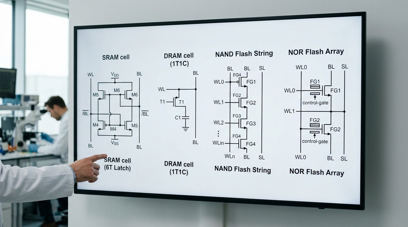
SRAM holds onto one bit using a 6-transistor (6T) latch, which is basically a tiny circuit where two flippers lock each other into a steady state. No refreshing needed at all. That steadiness, though, costs you room. Each cell needs six transistors, so it stays both big and pricey.
DRAM goes the other direction completely. One bit lives inside a single transistor with one little charge holder beside it, what folks call the 1T1C design.
That charge holder stores power kind of like a leaky bucket, and that’s exactly why DRAM has to refresh itself thousands of times every second. Fewer parts really means smaller cells.
According to Infineon’s 2023 memory data, an SRAM cell takes up 3,6× more area than a DRAM cell built on the same process. That one ratio essentially explains why your laptop carries approximately 16 GB[2] of DRAM but only 32,64 MB of SRAM cache sitting nearby.
How NAND and NOR Wire Their Cells Differently
Flash memory uses a floating-gate transistor, which is a transistor with an extra isolated gate that traps electrons to keep a bit even when the power is off. The wiring around those cells is what splits NAND apart from NOR.
- NAND links cells together in long series strings, sort of like Christmas lights wired end to end. This packs the cells in really tightly and gives you roughly 10–50× more bit density than DRAM at the system level, per Wikipedia’s flash memory overview. The catch, though, is that you can’t read just one cell on its own, so jumping around randomly stays slow.
- NOR wires each cell in parallel to the bit line instead. That extra metal lets the processor read any single byte instantly, which is perfect for boot code. The price you pay is lower density and a bigger chip area.
Quick practical tip from me. If your design runs code straight out of flash, what people call execute-in-place, then you really need NOR’s parallel cells. NAND strings just can’t handle byte-by-byte random reads fast enough to pull that off.
Volatility, Data Retention and What Survives Power Loss
Cut the power and two of these memories forget everything. SRAM and DRAM are volatile, they lose data the instant electricity stops.
NAND and NOR are non-volatile, holding data for years with no power at all. That single split decides whether a chip stores your photos or just your active calculations.
Volatile means “needs power to remember.” DRAM is the most forgetful.
Its 1T1C cell stores each bit as a tiny charge in a leaky capacitor, and that charge drains in milliseconds. To stop data from vanishing, the controller rewrites every cell thousands of times per second, a process called refresh.
DDR4 typically refreshes every cell within a 64-millisecond window. Stop refreshing, and the data is gone within milliseconds to seconds, per Infineon’s memory documentation.
SRAM is also volatile, but it doesn’t need refresh. Its 6-transistor latch holds the bit as long as power stays on. Pull the plug, though, and SRAM forgets just as fast as DRAM.
NAND and NOR play a different game. Both trap electrons in a floating gate, an insulated pocket that keeps charge without power.
That charge survives for 5 to 10 years at room temperature under rated conditions. This is why your phone keeps photos after the battery dies but loses whatever app was mid-load.
RAM vs ROM and the EEPROM Confusion
Here is where engineers trip up. The old label “ROM” (read-only memory) suggested permanent, unchangeable data. That definition broke decades ago.
- RAM (SRAM, DRAM) — volatile, fast, read and write freely, forgets on power loss.
- True ROM — non-volatile, written once at the factory, can’t change.
- EEPROM and NOR/NAND flash — non-volatile but rewritable, blurring the old ROM line entirely.
NOR flash is essentially flexible EEPROM built for code. Microcontrollers boot from it because the CPU can execute code straight from NOR without copying it to RAM first, a trick called execute-in-place (XIP). NAND can’t do this; it must load code into RAM first.
One practical warning: flash retention shrinks with heat and wear. A NAND chip rated for 10 years at approximately 25°C[3] may hold data only 1 year near its program/erase limit at approximately 55°C, per the JEDEC JESD47 endurance standards.
For long-archive storage, this retention drift matters far more than raw speed. Any honest comparison of DRAM, SRAM, NAND, NOR must weigh data survival, not just performance.

Speed, Latency and Bandwidth Compared With Real Numbers
Let me line these up by how fast you can actually reach the data, which we call access latency. SRAM is the quickest.
DRAM comes next, NOR sits somewhere in the middle, and NAND ends up last. SRAM grabs data in just a handful of nanoseconds, basically a tiny fraction of a second.
DRAM needs somewhere around 50 to 100 ns to do the same job. NOR reads things back in the range of tens to low hundreds of nanoseconds.
NAND trails far behind, landing in the tens to hundreds of microseconds.
And honestly, that last gap is enormous. The time it takes NAND to read something runs roughly 1,000 to 10,000 times slower than DRAM when you measure pure access time.
So why do NAND-based SSDs still feel quick to us? The answer is bandwidth, meaning how much data they can move at once.
A regular NVMe drive in 2025 can push 3 to approximately 7 GB[4]/s when it reads data laid out in order. But a single approximately 4 KB random read still pays the full microsecond cost of reaching that page.
Moving a lot of data quickly only hides the slow reaction time when you read large chunks in sequence.
| Memory | Read latency | Write/erase | Best access pattern |
|---|---|---|---|
| SRAM | 1–4 CPU cycles (sub-10 ns) | Same as read | Random, any address |
| DRAM | 50–100 ns | Similar to read | Burst rows, random rows costlier |
| NOR flash | Tens of ns | Milliseconds | Random read (execute-in-place) |
| NAND flash | Tens of µs | Hundreds of µs to ms | Sequential, page/block |
Really, the whole story comes down to random versus sequential access. SRAM and NOR let you reach any byte you want at the same speed, completely freely.
That ability is exactly why NOR can run execute-in-place (XIP). The processor pulls startup code directly out of NOR without first copying it into RAM. NAND simply cannot do that.
It has to read an entire page in one go, so it only performs well when the data arrives in order.
NOR reads fast but writes slowly. That happens because writing means changing the charge stored inside floating-gate cells, and erasing works in big blocks that take milliseconds to clear.
This lopsided behavior, with speedy reads but slow and painful writes, is why NOR ends up in boot ROMs rather than in places where you record constant data logs.
This Comparison of DRAM, SRAM, NAND, NOR latency makes matching the right memory to the right job something you really can’t skip.

Cost-Per-Bit and Density Economics
Cost ranking is simple: SRAM is the most expensive per bit, DRAM sits in the middle, and NAND is the cheapest. The gap is huge.
A bit of SRAM can cost roughly 100 times more than the same bit stored in NAND. That single fact drives almost every chip-design budget decision.
Why does SRAM cost so much? It comes down to cell size.
An SRAM cell uses a 6-transistor (6T) latch, six tiny switches holding one bit. A DRAM cell needs just one transistor and one capacitor (1T1C).
At the same process node, an SRAM cell runs 3,6× larger in area than a DRAM cell. Bigger cells mean fewer bits per wafer, and silicon is sold by area, not by bit.
NAND breaks the rules entirely. It stacks cells vertically instead of spreading them flat.
How 3D NAND Stacking Slashes Cost
Flat (planar) NAND hit a wall years ago, cells got too close and started leaking charge into each other. The fix was to build upward.
Modern 3D NAND stacks memory layers like floors in a skyscraper, with 2025-era production parts reaching 200+ layers in a single die. Each added layer packs more bits into the same wafer footprint, so cost per bit keeps dropping even when the flat dimension stops shrinking.
This stacking is also why NAND delivers roughly 10,50× higher bit density than DRAM at the system level. A smartphone might pair approximately 12 GB[5] of DRAM with approximately 512 GB of NAND in similar physical space.
| Memory | Cell structure | Relative cost per bit | Typical role driven by cost |
|---|---|---|---|
| SRAM | 6T latch (largest) | Highest (~100× NAND) | Small on-chip cache, kept tiny on purpose |
| DRAM | 1T1C | Mid-tier | Main working memory, tens of GB |
| NOR | 1 transistor, large array | Higher than NAND | Small code/boot storage |
| NAND | 3D-stacked floating gate | Lowest | Bulk storage, hundreds of GB to TB |
The practical lesson from this comparison of DRAM, SRAM, NAND, NOR: never use a costly memory where a cheap one fits. Designers cap SRAM cache at tens of megabytes precisely because scaling it to gigabytes would price the chip out of the market.
NOR sits above NAND in cost because its array layout wastes area, which is why engineers reserve NOR for small boot code and push everything bulky to NAND.
Endurance, Wear-Out and Long-Term Reliability
Will your memory survive a billion writes, or wear out in months? SRAM and DRAM endure practically unlimited read/write cycles in normal operation.
NOR flash handles roughly 100,000 erase cycles. NAND ranges from about 100,000 cycles for SLC down to a few thousand for the densest cells.
Endurance, not speed, often decides which memory lasts in heavy-write designs.
The split comes from physics. SRAM and DRAM store charge in transistors or capacitors that refresh harmlessly. Flash, by contrast, forces electrons through a thin oxide layer during every erase. That tunneling slowly damages the insulation. Eventually the cell can no longer hold a clean charge.
This is where the comparison of DRAM, SRAM, NAND, NOR splits into two camps. The volatile pair never wears from writing.
The non-volatile pair degrades with every program/erase cycle. According to a widely cited endurance breakdown on Electronics Stack Exchange, SLC NAND reached 50,000,100,000 cycles in 2024, while MLC/TLC dropped to around 3,000,5,000.
Endurance Ranked by Cell Type
| Memory | Write/Erase Endurance | Typical Use Impact |
|---|---|---|
| SRAM | Effectively unlimited | Cache writes never wear it |
| DRAM | Effectively unlimited | Refresh and writes are harmless |
| NOR flash | ~100,000 cycles | Fine for rarely-rewritten boot code |
| SLC NAND | 50,000–100,000 cycles | Industrial, high-write logging |
| TLC NAND | ~3,000 cycles | Consumer SSDs, needs wear leveling |
| QLC NAND | ~1,000 cycles | Read-heavy, archival storage |
Is SRAM More Reliable Than DRAM?
Yes, in two practical ways. Static RAM (SRAM) holds data in a 6-transistor latch that needs no refresh, so there’s no refresh-related corruption window.
DRAM stores each bit as charge in a tiny capacitor that leaks within milliseconds, forcing constant refresh. Miss a refresh and the bit flips.
SRAM also resists soft errors better in many designs because its latch actively holds state.
Both are still volatile. Neither keeps data after power loss. So “more reliable” here means fewer refresh-dependent failures, not data survival.
How Wear Leveling and ECC Extend Flash Life
Flash controllers fight wear-out with two tricks. Wear leveling spreads writes evenly across all blocks. Without it, a small log file rewritten daily would kill the same few blocks while the rest stay fresh. The controller remaps data so every block ages together.
The second defense is ECC (error-correcting code), which adds parity bits to detect and fix flipped cells. Modern TLC and QLC drives lean on LDPC (low-density parity-check) codes to recover bits that degrade as cells wear. Without strong ECC, QLC NAND’s ~1,000-cycle rating would be unusable.
One field insight: enterprise SSD datasheets quote endurance as DWPD (drive writes per day) over a warranty term. A 1 DWPD drive rated for 5 years tolerates writing its full capacity daily for that period.
Match this number to your real write workload before buying, many teams overpay for high-DWPD drives on read-heavy jobs. For deeper reading, see the Wikipedia entry on flash memory.
Bottom line for designers: if your application rewrites the same address millions of times, choose SRAM, DRAM, or SLC NAND. Reserve QLC for data you write once and read often.
A Decision Flowchart for Choosing the Right Memory
Match the job to the memory, not the other way around. Need single-cycle access glued to your processor?
Use SRAM. Need gigabytes of cheap working space?
Use DRAM. Storing the boot code that runs before anything else loads?
NOR flash. Holding photos, apps, and operating system files?
NAND. This entire comparison of DRAM, SRAM, NAND, NOR collapses into four clear if-then rules once you know your constraint.
Start by asking one question: does the data need to survive a power cut? If no, you’re choosing between SRAM and DRAM. If yes, you are choosing between NOR and NAND.
The if-then selection matrix
| If your need is… | Then pick… | Why it wins here |
|---|---|---|
| CPU L1/L2/L3 cache, sub-10 ns latency | SRAM | 1–4 cycle hits; no refresh needed |
| Main system memory, tens of GB | DRAM | Cheapest volatile bit at high density |
| Boot/firmware code that runs in place | NOR flash | Fast random reads (tens of ns), reliable |
| Mass storage: OS, files, media | NAND flash | 10–50× higher bit density than DRAM |
Real designs blend all four. A typical smartphone in 2024 carried tens of MB of SRAM cache inside the SoC, approximately 16,24 GB[6] of LPDDR5 DRAM for apps, and approximately 128 GB[7] to approximately 1 TB of NAND for storage.
NOR often hides in the boot ROM, holding the tiny first-stage loader because it supports execute-in-place (XIP), running code directly from flash without copying it to RAM first.
Practical rule engineers learn the hard way: never use NAND for boot code that must run before a RAM controller initializes. NAND can’t do reliable random reads byte-by-byte. That is NOR’s exact job.
Common Selection Mistakes and Counterintuitive Trade-offs
The most expensive memory mistakes come from picking the right family for the wrong reason. Engineers grab NAND because it’s cheap, then discover the CPU can’t run code from it. Or they over-spec SRAM where DRAM would have done the job for a fraction of the cost.
Here are the errors I see wreck real projects.
Trying to execute code directly from NAND
NAND can’t do execute-in-place (XIP), where the processor fetches instructions straight from memory. NAND is read page-by-page, not byte-by-byte, so there’s no random access to individual words.
NOR flash supports XIP because it offers true random reads at tens to low hundreds of nanoseconds, which is why boot ROMs and microcontroller firmware live in NOR. The fix for NAND systems: copy code into DRAM at boot, then run from there.
Ignoring NAND endurance in write-heavy logging
This one kills devices in the field. TLC NAND survives only about 3,000,5,000 program/erase cycles, versus 50,000,100,000 for SLC, per endurance data on Electronics Stack Exchange.
A data logger writing the same block every few seconds can wear out cheap TLC in months. Wear leveling spreads writes across the chip, but it only delays the problem if your logging volume is high.
Over-specifying SRAM
SRAM cells are 3,6× larger than DRAM cells at the same process node, which makes SRAM far pricier per bit. Need approximately 8 GB[8] of working memory? Use DRAM. Reserve SRAM for the small, latency-critical buffers where sub-10 ns access actually matters.
Where pairings and HBM fit
| Pairing | Why it works |
|---|---|
| DRAM + NAND | NAND stores bulk data; DRAM holds the active working set and runs code |
| HBM + standard DRAM | HBM stacks DRAM dies for huge bandwidth in GPUs and AI accelerators |
| NOR + DRAM | NOR boots and stores firmware; DRAM handles runtime |
This is the core lesson of any honest comparison of DRAM, SRAM, NAND, NOR: each memory has one job it does well. Force it into the wrong role and you pay in cost, lifespan, or a system that won’t boot.
Frequently Asked Questions
Short answers tied to real scenarios, no hedging. These three questions drive most of the confusion in any comparison of DRAM, SRAM, NAND, NOR.
Is DRAM or NAND better?
Neither. They do opposite jobs. DRAM holds your active working data; NAND stores files when the power is off. A smartphone needs both: LPDDR5 DRAM for running apps, NAND for the approximately 128 GB to approximately 1 TB[9] of photos and videos.
The speed gap is brutal. NAND is roughly 1,000,10,000× slower in raw access than DRAM, per flash memory data on Wikipedia. Use NAND for capacity. Never use it as live working memory.
Which is better between DRAM and SRAM?
SRAM wins on speed, DRAM wins on capacity and price. SRAM hits sub-10 ns latency and sits on-chip as L1/L2/L3 cache, usually approximately 32,64 MB in a desktop CPU. DRAM runs 50,100 ns but scales to tens of gigabytes off-chip.
The reason is the cell. SRAM uses a 6-transistor (6T) latch, making each cell 3,6× larger than DRAM’s 1-transistor/1-capacitor (1T1C) design, according to Infineon. That size tax is why you can’t build gigabytes of SRAM affordably.
Is SRAM more reliable than DRAM?
For data integrity, yes. SRAM stores bits in a stable latch and doesn’t need refreshing. DRAM leaks charge from its capacitor and must refresh thousands of times per second, miss that, and the data vanishes. Both endure practically unlimited writes, so neither wears out like NAND.
Choosing Your Memory With Confidence
One rule covers most projects: put code and tiny buffers in SRAM, run active programs in DRAM, store firmware in NOR, and dump bulk data into NAND.
The four-way comparison of DRAM, SRAM, NAND, and NOR always comes down to a trade between speed, cost, density, and whether data must survive a power cut.
Here is the recap in one table. Read it as a ranking, not a verdict, your workload breaks the tie.
| Memory | Best Role | Volatility | Key Limit |
|---|---|---|---|
| SRAM | On-chip cache (L1/L2/L3) | Volatile | 6T cell, 3–6× larger area than DRAM |
| DRAM | Main working memory | Volatile | Needs constant refresh; loses data in milliseconds |
| NOR | Boot code, firmware | Non-volatile | Low density; slow writes |
| NAND | Bulk storage (SSD, mobile) | Non-volatile | Wear-out; TLC endures ~3,000–5,000 cycles |
Density tells you why this split exists. By 2024, single-package NAND in phones and SSDs ran approximately 128 GB[10] to approximately 1 TB, roughly 10,50× denser than DRAM at the system level. You can’t cheat that gap with clever design.
Your next step is concrete. Write down three numbers for your project: required access latency, total capacity, and whether data must persist without power.
Match those against the table above. If two memory types fit, pick the cheaper per-bit option unless write endurance fails your duty cycle.
That single checklist prevents most mismatches before you order a single chip.