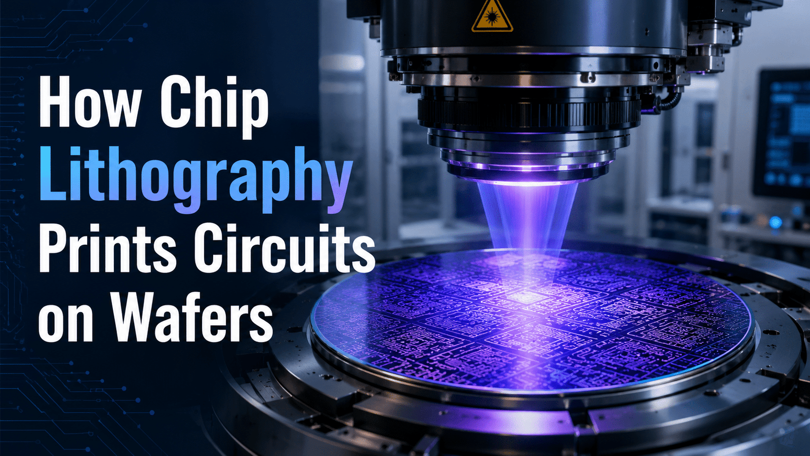
The photolithography process in chip making prints circuit patterns onto silicon wafers using light, a patterned mask, and a light-sensitive coating called photoresist. Advanced EUV systems use 13.5 nm wavelength light to pattern features for leading-edge nodes such as 5 nm and below as of 2026 (ASML). A single modern chip repeats this print-and-etch cycle 80 to 100 times across 30 or more mask layers, building circuits layer by layer at a scale measured in billionths of a meter.
The photolithography process in chip making is essentially a printing step: it copies a circuit blueprint onto a wafer using light, light-sensitive chemicals, and precise masks.
Picture a stencil and a can of spray paint. The mask acts as the stencil, the light acts as the paint, and a chemical coating called photoresist captures the pattern. A single modern chip goes through this print-and-etch cycle 80 to 100 times, building circuits layer by layer.
This guide breaks down each step, the machines behind it, why nanometer precision matters, and where the technology is headed.
Quick Takeaways
- EUV lithography uses 13.5 nm light to pattern 5 nm and below nodes.
- Modern chips need 30+ mask layers, each repeating coat-expose-develop-etch cycles.
- A single chip undergoes the print-and-etch cycle 80 to 100 times.
- The mask acts as stencil, light as paint, photoresist captures the pattern.
- Photolithography precision directly determines how small your transistors can be.
What Photolithography Does in Chip Making
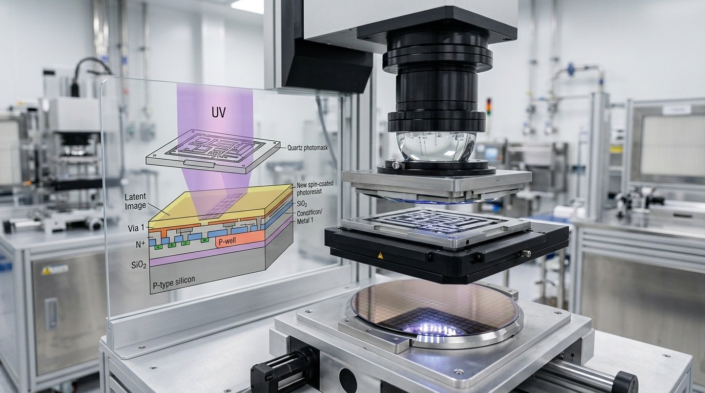
The photolithography process in chip making prints circuit patterns onto silicon wafers using light, a patterned mask, and a light-sensitive coating called photoresist. Light shines through the mask, hits the resist, and copies the design onto the wafer at a scale measured in billionths of a meter.
This single technique decides how small your transistors can be.
Here is the part most explainers skip: one pass is never enough. A modern chip needs 30 or more separate mask layers, and each layer runs its own coat,expose,develop,etch cycle.
Logic nodes and dense memory can push that count past 60 or 70. Every layer stacks another piece of the circuit,wiring, transistors, contacts,on top of the last.
Why repeat it so many times? A chip is a 3D building, not a flat drawing. You can’t print billions of transistors plus their wiring in one shot. So fabs interleave etching, ion implantation, and deposition between lithography steps, building structure by structure.
Lithography also sets the floor on transistor size. The smallest feature you can print scales with the light’s wavelength.
That’s why the industry moved from older 365 nm light to deep ultraviolet, then to EUV at 13.5 nm wavelength, which enables 5 nm-class nodes and below. Shorter light, sharper patterns.
Practical reality: if lithography is off by even a few nanometers on one layer, every layer above it can fail. That dependency makes it the most expensive and most closely monitored step in the whole fab.
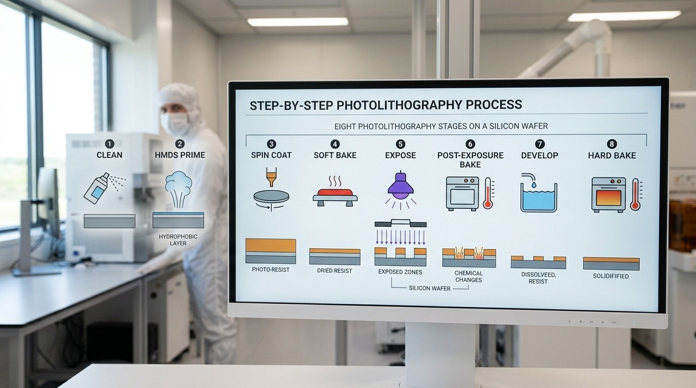
The Eight Core Steps from Wafer to Patterned Resist
The photolithography process in chip making takes a plain silicon wafer and turns it into a patterned surface, and it happens across eight ordered steps. Those steps are clean, prime, coat, soft bake, align and expose, post-exposure bake, develop, and hard bake.
Each one gets the light-sensitive coating ready for the next. Skip even a single step, and the pattern just fails.
Clean and prime. First, the wafer gets stripped of stray particles and that thin natural oxide layer. Then a vapor called HMDS coats the surface, which is basically a chemical that helps things stick.
Without it, water clings to the silicon and the coating peels right off during development. HMDS makes the wafer push water away, so the coating holds on tight.
Coat and soft bake. Liquid photoresist, which is the light-sensitive coating, gets spun on at thousands of spins per minute to make a film that’s often thinner than one micrometer. After that, the soft bake drives out the leftover solvent.
This step runs between roughly 60 °C and 100 °C. Run it too cool and trapped solvent leaves bubbles. Run it too hot and the coating hardens early, so it won’t develop cleanly later on.
Align, expose, post-exposure bake. A stepper, which is the machine doing the positioning, lines up the mask. Then UV light actually prints the pattern. The post-exposure bake smooths out the little ripples in the coating’s sidewall, sharpening up the line edges before development happens.
Develop and hard bake. Developer washes away the parts that dissolve, and the pattern shows up. Then the hard bake locks everything in at about 120,180 °C for up to 20,30 minutes, toughening the coating against the etching step that comes next.
Cut corners on this bake, though, and the lines wear away during etching. That essentially ruins how clean the line edges turn out.
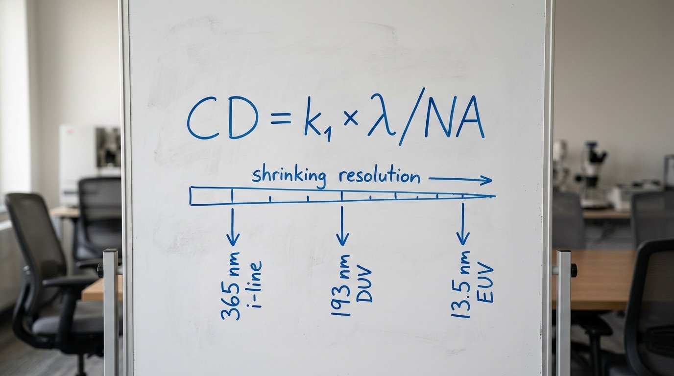
Why Resolution Is Physically Hard to Improve
Resolution in the photolithography process in chip making is governed by one equation: CD = k1 × λ / NA. Smaller features need either shorter wavelength light (λ), a bigger lens aperture (NA), or a tighter process factor (k1).
All three hit physical walls. You can’t just push a slider and print smaller circuits.
CD means critical dimension, the smallest line or gap you can print. Break the equation into its three levers:
- λ (wavelength): Shorter light prints finer lines. The industry jumped from i-line at 365 nm to deep ultraviolet (DUV) at 248 nm and 193 nm, then to extreme ultraviolet (EUV) at 13.5 nm. ASML’s EUV systems use that 13.5 nm wavelength to pattern 5 nm logic nodes and below.
- NA (numerical aperture): A measure of how much light the lens collects. Higher NA bends more light to focus tighter. Dry 193 nm lenses topped out near NA 0.93. Water immersion pushed it to 1.35.
- k1 (process factor): A coefficient set by resist chemistry and tricks like phase-shift masks. The theoretical floor is about 0.25 for a single exposure.
Here is the trap. Going from 193 nm DUV to 13.5 nm EUV shrinks λ by roughly 14 times, the only lever with real headroom left.
The catch: glass lenses absorb 13.5 nm light, so EUV needs vacuum chambers and mirrors instead of lenses, a complete machine redesign rather than a tweak.
Shrinking k1 below 0.25 with one exposure is impossible by physics. That’s why fabs split patterns across several exposures, the focus of the next section.
DUV, Immersion, and EUV Lithography Trade-Offs
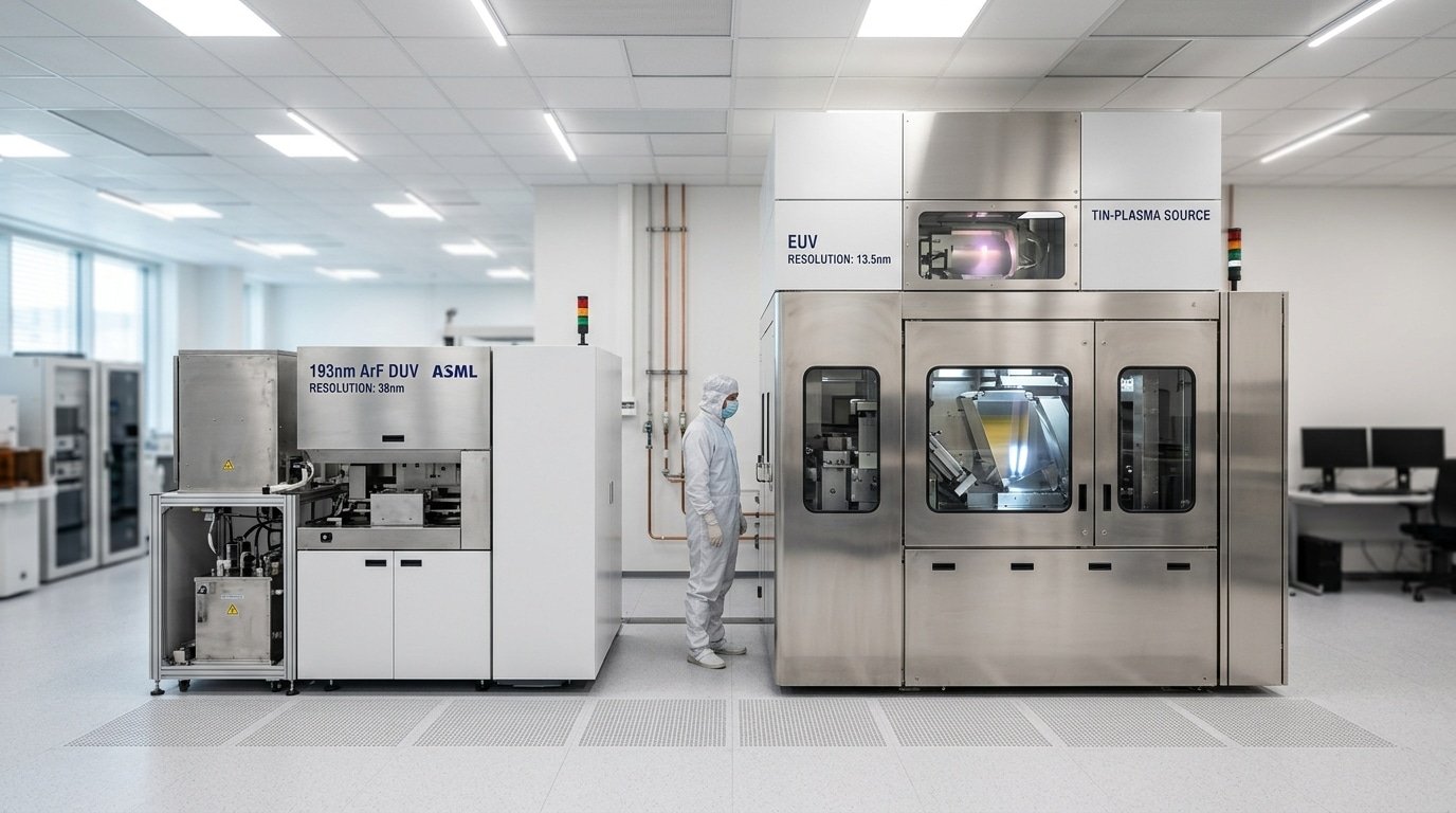
No single light source wins in every situation. Dry 193nm DUV, which uses light with a 193 nanometer wavelength in open air, can print features down to roughly 65nm half-pitch. And it stays cheap to run.
Immersion 193nm goes further, reaching about 38nm by adding a thin layer of water between the lens and the wafer. EUV uses 13.5nm light, which is a much shorter wavelength, to pattern 5nm-class logic chips and even smaller ones.
Each technology really owns its own slice of the cost and chip-size range.
So why does one EUV scanner cost over 150 million dollars? The short answer is that 13.5nm light simply can’t travel through air or glass at all.
It needs a vacuum chamber to work in, mirrors instead of lenses to bounce the light around, and a tin-droplet plasma source that gets struck by a high-power laser to actually create the photons. That hardware is brutally hard to build and keep working.
| Technology | Wavelength | Min half-pitch | Throughput (wph) | Best node fit |
|---|---|---|---|---|
| 193nm dry DUV | 193 nm | ~65 nm | 200+ | 90–45 nm, older layers |
| 193nm immersion | 193 nm + water | ~38 nm | ~150–250 | 28–7 nm via multi-patterning |
| EUV | 13.5 nm | ~13 nm | ~150–185 | 5 nm and below, critical layers |
Here is the money side that nobody tends to explain. Even at 5nm, most of the mask layers in the photolithography process in chip making still run on the older DUV tools.
EUV gets saved only for the very tightest layers, the ones where doing multi-patterning with immersion would need four or more masks instead. Each extra mask adds cost. It also adds the risk that the layers won’t line up properly.
So fabs mix their tools together. A 7nm flow might use a single EUV pass to replace three immersion passes, which saves steps even though the scanner is pricey.
But for a memory chip or a power chip with looser, more relaxed features? Buying EUV would just burn money for no benefit at all.
In my experience, you match the tool to the chip generation, not to the hype around it.
Multi-Patterning and Why One Exposure Is Not Enough
When a layer needs features tighter than one exposure can print, fabs split that layer across two or more masks. This is multi-patterning.
⚠️ Common mistake: Assuming one lithography pass prints a whole chip. In reality, a modern chip repeats the coat-expose-develop-etch cycle 80 to 100 times across 30+ mask layers. This happens because circuits are built in stacked layers, not one flat image, and each layer needs its own mask and alignment. The fix: think of photolithography as 30+ sequential print runs, each requiring nanometer-level overlay accuracy.
Before EUV at 13.5 nm wavelength matured around 2019, it was the only way to reach 20 nm, 14 nm, and 10 nm nodes using 193 nm immersion light.
Three methods dominate the photolithography process in chip making:
- LELE (Litho-Etch-Litho-Etch): Print half the lines on mask A, etch them, then print the other half on mask B in the gaps. Two full exposures and two etches make one dense layer. Doubles the patterning cost for that layer.
- SADP (Self-Aligned Double Patterning): Print wide “mandrel” lines, then grow a thin spacer film on their sidewalls. Strip the mandrels and the spacers become the real pattern. One exposure, but extra deposition and etch steps. SADP halves the pitch.
- SAQP (Self-Aligned Quadruple Patterning): Repeat the spacer trick twice. One exposure yields four lines per original line. Intel used SAQP for its fin patterning at the 14 nm and 10 nm nodes.
The cost is real. A single LELE layer needs two reticles instead of one, and reticles for advanced nodes run hundreds of thousands of dollars each.
Cycle time also stretches. Each extra litho-etch loop adds hours of tool time and more chances for overlay error, which the next section explains.
So why did fabs pick this pain? Because waiting was worse. With EUV scanners costing over $150 million each and supply scarce, multi-patterning let companies ship 10 nm chips years before EUV could deliver volume. Today many layers stay on DUV multi-patterning when EUV would be overkill.
Overlay, Edge Placement Error, and Alignment Accuracy
Printing a sharp pattern is only half the job. Each new layer must land precisely on top of the layers already built.
That stacking accuracy is called overlay, and on leading-edge nodes the overlay budget shrinks to roughly 2,3 nanometers. Miss it, and the chip fails even if every feature is crisp.
Why so tight? A modern chip stacks 30 or more mask layers, and each must connect to the one below through tiny holes called vias.
If a metal line drifts a few nanometers from the via it should touch, the connection breaks. The wafer looks perfect under a microscope.
The transistor still dies.
Edge placement error (EPE) is the metric that ties this together. EPE measures the gap between where a feature edge actually sits and where the design says it should be. It combines two errors: the line’s own size variation plus the overlay drift between layers.
Multi-patterning makes EPE worse because errors stack. Split one layer across four exposures, and each exposure adds its own placement error.
Those errors add in quadrature, so the total grows with each extra mask. This is why fabs running 5nm logic spend heavily on alignment marks etched into the wafer that the scanner reads before every exposure.
One practical rule engineers follow: budget overlay at about one-fifth of the smallest feature. For a 13.5nm EUV-printed feature, that leaves almost no room for thermal drift or wafer warp. A wafer heated unevenly during a bake can expand enough to blow the entire budget.
Common Lithography Defects and Yield Loss
The most common lithography defects in chip making are bridging, line collapse, missing contacts, focus and dose errors, and particle contamination. Each one traces back to a specific root cause, wrong exposure energy, a dirty reticle, a poorly tuned bake, or mechanical stress in the resist.
Catching the defect type tells the engineer where to look first.
Bridging happens when two lines that should stay separate touch each other. The usual culprit is overexposure or a focus error that smears the printed edge.
Line collapse is the opposite problem of geometry: tall, skinny resist lines fall over during development because the rinse water pulls them sideways. A line taller than about 4 times its width is at high risk.
Missing contacts, open holes that never print, often come from underexposure or particle blockage on the reticle. Since a modern chip can need 30 or more mask layers, a single bad contact layer can scrap the whole device.
Fab engineers triage yield drops with a quick decision table:
| Defect Seen | Likely Root Cause | First Fix to Try |
|---|---|---|
| Lines bridging together | Overdose or defocus | Lower dose, recheck focus offset |
| Resist lines fallen over | Aspect ratio too high | Thinner resist, gentler rinse |
| Missing contact holes | Underdose or reticle particle | Inspect reticle, raise dose |
| Random spot defects | Airborne particle | Check track filters, clean stage |
A practical tip: when defects cluster at the wafer edge, suspect coat uniformity, not the scanner. Edge resist is thicker, so dose lands off-target there first.
Metrology and Process Control That Catch Problems Early
After develop, every wafer goes through inspection before it touches an etch tool. Fabs measure critical dimension (CD), check overlay, and scan for defects at this gate, called after-develop inspection (ADI).
The goal is simple: catch a bad lithography step while the resist can still be stripped, not after etch makes the error permanent.
CD-SEM (critical-dimension scanning electron microscope) measures line widths down to the nanometer. A typical 5 nm logic layer might hold its CD to a target with a 3-sigma window of only a few nanometers.
If lines print too wide or too narrow, the tool flags it before the pattern locks in.
Overlay metrology checks how well the new layer lands on the layer below. Tools read special alignment marks and report shift in x and y.
Since EUV systems at 13.5 nm wavelength print 5 nm and smaller features, overlay budgets here run tight, often under 2 nm for the most demanding layers.
Here is where the photolithography process in chip making gets a second chance. Resist is just patterned polymer, not etched silicon. If ADI shows the CD or overlay is out of limit, engineers can strip the resist and re-coat, re-expose, re-develop the same wafer. This is called rework.
The rework rule of thumb:
- Rework if the defect lives only in resist and the layer below is undamaged.
- Scrap if etch already ran, or if rework would push that layer past its rework count limit (often capped at 2–3 cycles to avoid film damage).
One pitfall: too many rework cycles thin the underlying oxide and degrade later overlay. Smart fabs track rework rate as a yield signal, not just a fix.
Frequently Asked Questions
Short answers to the questions searchers ask most about chip lithography.
What’s the photolithography process in chip making?
It’s the step that prints circuit patterns onto a silicon wafer using light. A patterned mask blocks or passes light, which changes a light-sensitive coating called photoresist.
The process is repeated 30 or more times for a single chip, since each layer needs its own coat, expose, develop, and etch cycle.
How does chip lithography work step by step?
A standard sequence runs: clean the wafer, spin on photoresist, soft-bake to drive out solvent, expose through the mask, post-exposure bake, develop, then hard-bake. Each step has tight limits.
The soft-bake alone heats the wafer to roughly 60,100 °C, per process overviews. Skip or rush one step and the printed line wanders off target.
What’s the difference between lithography and etching?
Lithography prints a soft pattern in resist using light. Etching is the next step: it carves that pattern into the material below by removing exposed areas with chemicals or plasma.
Think of lithography as drawing the stencil, and etching as cutting through it. Resist is temporary; the etched layer stays.
Does EUV fully replace DUV?
No. EUV at 13.5 nm prints the tightest features for 5 nm nodes and below, but DUV at 193 nm and 248 nm still handles most layers on any chip.
A single advanced chip uses both. EUV tools cost far more, so fabs reserve them for the few layers that truly need them.
Key Takeaways on How Lithography Prints Circuits
The photolithography process in chip making is hard for three reasons stacked on top of each other: resolution is capped by physics, alignment drifts between layers, and tight features force fabs to split one pattern across several exposures. Get any one wrong and the chip fails.
Master all three and you can print billions of transistors on a fingernail-sized die.
Resolution is bounded by the Rayleigh relation, feature size scales with wavelength divided by numerical aperture. That math is why the industry jumped from 365 nm i-line light to 193 nm DUV, then to 13.5 nm EUV for 5 nm logic nodes and below.
Shorter light prints smaller lines, but each shift took decades of optics work.
Overlay drift is the quiet killer. Each layer must land on the one beneath it within a few nanometers. Edge placement error stacks across layers, so a fab that ignores overlay budget loses yield even when every single exposure looks sharp.
Multi-patterning is the workaround when one shot can’t resolve the pitch. Splitting a layer doubles or triples the coat,expose,develop,etch cycles, and a finished chip can already need 30 or more separate mask layers. More steps means more chances for defects and higher cost.
Where to go deeper:
- EUV physics — vacuum optics, tin-droplet plasma sources, and pellicle limits
- Mask making — reticle defect repair and why one bad mask scraps every wafer
- Fab integration — how litho ties into etch, implant, and deposition loops
Treat lithography as a yield system, not a single tool. The fabs that win optimize the whole chain.
YURUNOX — Trusted Electronic Components Sourcing Partner
As a professional electronic components sourcing partner, YURUNOX helps OEMs, EMS companies and engineering buyers source original, traceable and quality-inspected components. Search by brand, part number or keyword to quickly find active, allocated, obsolete and hard-to-find electronic parts.
- ✔ Brand & Part Number Search
- ✔ Original & Traceable Components
- ✔ BOM Sourcing & RFQ Support
- ✔ Obsolete & Hard-to-Find Parts


