EUV lithography for chip fabrication uses extreme ultraviolet light at a 13.5-nanometer wavelength to pattern the most intricate layers of advanced logic and memory chips, and it costs a fab far more than the sticker price suggests. A single standard NA 0.33 scanner runs approximately $150–200 million, while newer High-NA 0.55 tools exceed approximately $380 million each.
Installation, a Class 1 cleanroom (~1,000 sq ft), and a 1-megawatt power draw roughly double the real outlay, pushing fabs toward a five-to-seven-year payback window per machine.
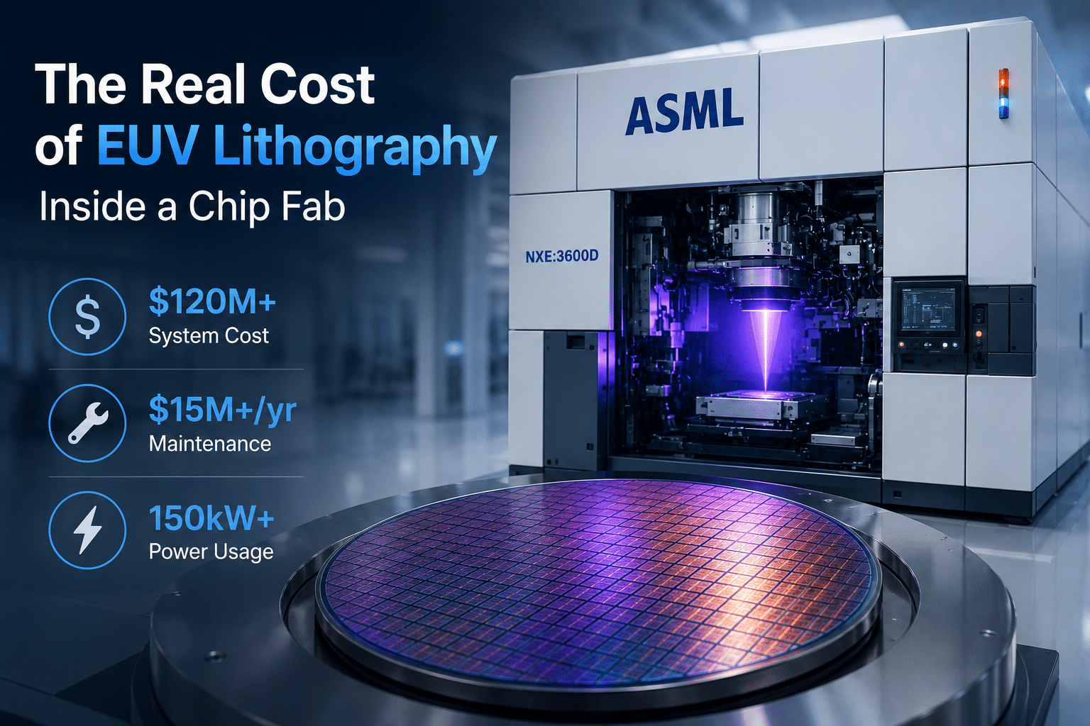
So what does EUV lithography for chip fabrication actually cost a fab once you add power, maintenance, and the rare-earth supply chain behind every exposure? The short answer: far more than the sticker price suggests.
Quick Takeaways
- Standard EUV scanners cost approximately $150–200M; High-NA tools exceed approximately $380M each.
- Add installation, cleanroom, and power to roughly double the sticker price.
- Each EUV tool draws 1 megawatt; 20 tools equal a small town.
- Budget 3–6 months for installation and qualification per scanner.
- Target a five-to-seven-year payback window before a tool turns profitable.
What EUV Lithography Actually Costs a Chip Fab
A single standard EUV scanner costs approximately $150,200 million per unit, while the newer High-NA tools push past approximately $380 million each.
The sticker price is just the start: installation, the dedicated cleanroom, and supporting infrastructure roughly double the real outlay,which is why fabs target a payback window of five to seven years before a tool turns profitable.
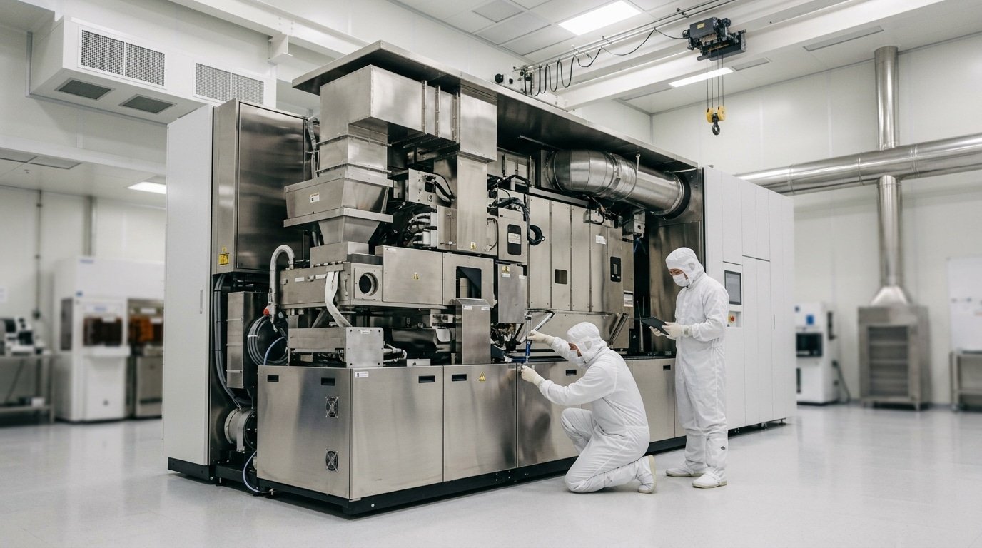
Here is what nobody tells you about EUV lithography for chip fabrication: the scanner alone weighs around 180 tons and ships in roughly 40 freight containers. According to ASML, individual EUV systems cost on the order of approximately $200 million per unit.
Bolting one into a fab takes three to six months and a dedicated team of installation and qualification engineers.
The hidden costs stack up fast:
| Cost item | Approximate figure |
|---|---|
| Standard NA 0.33 scanner | approximately $150–200M |
| High-NA 0.55 scanner | approximately $380M+ |
| Cleanroom space per tool | ~1,000 sq ft (Class 1) |
| Power draw, single tool | ~1 megawatt |
| Installation + qualification | 3–6 months |
That 1-megawatt draw matters. A fab running 20 EUV tools burns roughly 20 megawatts,power equal to a small town,mostly to vaporize tin droplets and cool the optics.
The cleanroom must hold Class 1 purity,fewer than one particle per cubic foot,because a single 20-nanometer speck, smaller than a virus, ruins a wafer.
Fabs don’t run every layer on EUV. They reserve it for the most critical patterning steps and lean on cheaper deep ultraviolet (DUV) tools elsewhere, a trade-off explored in the cost-per-wafer math ahead.
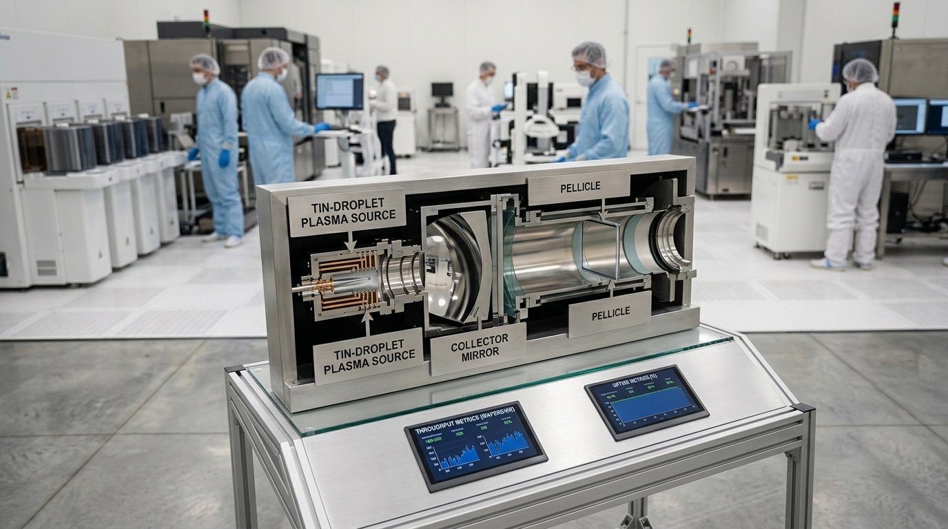
How EUV Patterns a Wafer Using 13.5nm Light
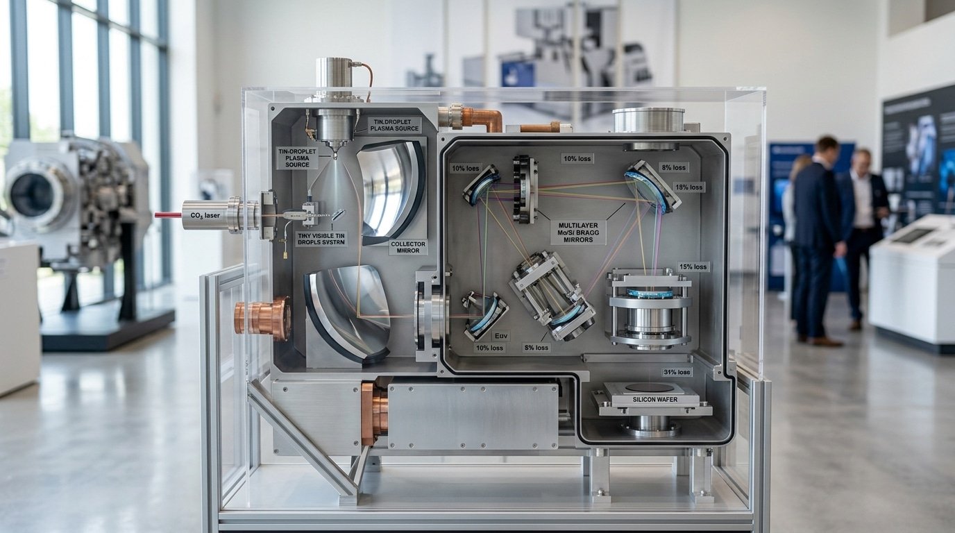
EUV lithography for chip fabrication actually starts with a tiny explosion. A powerful CO₂ laser fires at 20,30 micrometer tin droplets around 50,000 times every single second. That’s a lot of shots.
Each hit turns the tin into a glowing cloud, basically plasma, that shines at exactly 13.5 nanometers. That light then travels toward the wafer. And it loses money at every single bounce along the way.
Here is the harsh physics problem we run into. Almost every material on Earth just soaks up 13.5nm light, which means ordinary glass lenses are completely useless here.
So instead, the tool depends on multilayer Bragg mirrors, which are essentially stacks of alternating molybdenum and silicon (Mo/Si) layers, each one only a few atoms thick. These mirrors bounce back roughly 70% of the EUV light coming in.
The remaining approximately 30% just disappears as heat.
Now think about stacking all those losses together. A typical EUV scanner uses 10 or more mirrors sitting between the source and the wafer.
With each one keeping only about 70%, the math piles up really fast. Take 0.70 to the tenth power and you find barely 2,approximately 3% of the original light actually reaches the photoresist.
Every photon you waste has to be replaced by burning more laser power. That is the direct connection between losing light and the 1-megawatt power bill we talked about in the section before.
So that’s why source power limits how much you can run. Over time, tin debris coats the collector mirror, which drags the efficiency down and forces you to stop for maintenance.
The whole light path also runs in a near-perfect vacuum, since air molecules absorb 13.5nm light too. Pumping and keeping that vacuum stable adds genuine operating cost on top.
So here’s the practical takeaway. Fabs save EUV only for the most critical chip layers, because each pass over a wafer, running at roughly 2,approximately 3% optical efficiency, is honestly too expensive to spend on simple patterns.
EUV vs DUV Multi-Patterning, the Cost-Per-Wafer Math
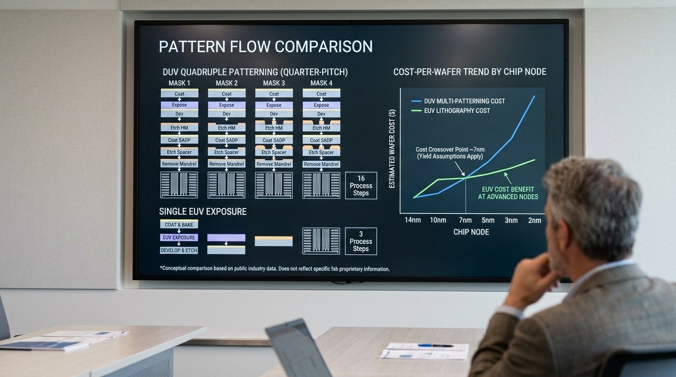
Below the 7nm node, single-exposure EUV beats quadruple-patterning DUV on cost per wafer,even though an EUV scanner costs four to five times more than a DUV tool. The crossover happens because DUV needs four separate exposures to print one tiny layer, and each extra step adds masks, time, and chances to ruin the wafer.
Here is the math foundries actually run. To print a layer at the 7nm node, deep ultraviolet (DUV) lithography,the older 193nm light that came before EUV,requires self-aligned quadruple patterning, or SAQP. One EUV pass replaces all of that.
| Metric (per critical layer) | DUV Quad-Patterning | Single-Exposure EUV |
|---|---|---|
| Mask layers needed | 4 | 1 |
| Process steps (etch, deposit, clean) | ~30+ | ~8 |
| Cycle time per layer | Several days | Under one day |
| Defect-injection points | High (each step risks particles, overlay error) | Low |
Every extra DUV mask costs money, and every one of those 30-plus etch steps is a fresh chance for a particle to land and kill the chip.
That’s why foundries use EUV lithography for chip fabrication only on the most critical layers, while less demanding layers stay on cheaper DUV.
The pitch tells the story. EUV reaches features below 20nm in a single shot, around 13nm half-pitch in resist. DUV physically can’t, so it splits the pattern into four pieces. Stack enough pieces and the labor wins,EUV pulls ahead at 7nm and stays ahead at 5nm and 3nm.
Throughput, Uptime, and the Hidden Bottlenecks in High-Volume Manufacturing
A modern EUV scanner prints 160,220 wafers per hour when it is moving at full speed, and the people running these factories aim for the machine to be working close to 90% of the time. That final approximately 10% is where the numbers turn really painful.
Picture a tool that costs approximately $200 million sitting idle one day a week. It loses millions in wafers it could have started but never did.
How much it can handle per hour really comes down to source power, meaning how strong the light is. To reach 200 or more wafers per hour, the laser-produced plasma source has to keep up around 250 watts of EUV power at the intermediate focus.
When power drops, each wafer needs a longer exposure time, and that directly lowers how many wafers you get through. ASML’s EUV systems use 13.5nm light made from tin-droplet plasma (ASML). Honestly, that source is the single biggest factor in what actually comes out the other end.
The capacity these factories paid for on paper gets quietly eaten away by maintenance that older DUV tools never even needed:
- Collector mirror cleaning — over time, tin debris coats the collector mirror and lowers how much light it reflects. Swapping it out means the tool is offline for hours.
- Pellicle handling — the thin protective film sitting over the mask is fragile, and it has to survive intense EUV power. If that film tears, the whole run is scrapped.
- Source maintenance — the droplet generators clog up, and tin contamination forces cleaning cycles that have to be scheduled in.
Here is the trap. A tool rated for 200 wafers per hour almost never delivers a full 200 across an entire quarter.
So engineers track something called “effective throughput,” which basically folds in all that downtime. A tool that is available approximately 90% of the time and running at 200 wph effectively prints closer to 180.
That lost output is exactly why factories save EUV lithography for chip fabrication for the most critical layers. Every single minute on an EUV tool is just too valuable to waste on layers that a cheaper DUV scanner could pattern instead.
Defectivity and Yield, Where EUV Quietly Loses Money
EUV’s biggest hidden cost isn’t the scanner,it’s the wafers you throw away. Stochastic defects, random pattern failures caused by too few photons hitting each tiny feature, can wreck yield on the most critical layers.
⚠️ Common mistake: Budgeting only the approximately $150–200M sticker price when planning an EUV tool purchase. This happens because installation, a Class 1 cleanroom, and a 1-megawatt power draw are easy to overlook—yet they roughly double the real outlay and stretch the five-to-seven-year payback window. The fix: Model total cost of ownership, including the 3–6 month qualification and ongoing power, before committing capital.
At advanced nodes, a single percent of yield loss on a approximately $200-million tool can erase millions in profit per month.
Here’s the physics. EUV’s 13.5nm light carries about 14 times more energy per photon than older 193nm DUV light.
To deliver the same exposure dose, EUV uses far fewer photons per pixel. Fewer photons means more statistical “noise”,like trying to spray-paint a coin and missing spots.
Some contact holes don’t open. Some lines merge or break.
These are stochastic defects, and they scale brutally as features shrink.
The trade-off is cruel. To cut defects, you raise the resist dose (more photons).
But higher dose slows throughput and raises cost per wafer. Lower dose speeds things up but worsens line-edge roughness (LER),the jagged wobble along a line’s edge.
Technical reviews report line-width roughness around 3,4 nm in EUV exposures, which becomes a yield killer when half-pitch drops near 13nm.
Then there’s the pellicle,a thin protective film over the mask. EUV pellicles absorb light, and real-world membranes have historically cut transmission to roughly 80,approximately 90%.
Every percent lost forces longer exposures, which slows the tool and raises dose. That dose penalty stacks on top of the stochastic problem, which is why EUV lithography for chip fabrication runs only on the few layers where the resolution is truly worth the yield risk.
Practical tip: fabs fight stochastics with smart resists, defect inspection on every critical layer, and dose tuning per feature type,not one global setting.
Why ASML Holds a Monopoly and What That Does to Pricing
ASML is the only company on Earth that sells EUV scanners. As of 2026, it remains the sole commercial supplier, with each system costing around $200 million. No rival ships a competing tool. That monopoly is why fabs pay what they pay and wait years for delivery.
The lock-in runs deeper than ASML’s own factory. The machine depends on two partners no competitor can copy.
Carl Zeiss SMT builds the multilayer Bragg mirrors,stacks of dozens of nanometer-thin layers that reflect 13.5nm light, since ordinary glass lenses just absorb it. Cymer, which ASML bought in 2013, makes the laser-produced plasma light source that vaporizes tin droplets.
Three decades of joint R&D fused these three into one supply chain.
What does single-supplier power do to a fab’s wallet and calendar?
- No price competition. With zero alternatives, EUV lithography for chip fabrication carries list prices set by ASML alone. A standard scanner runs approximately $150–200 million; High-NA tools exceed approximately $380 million.
- Multi-year backlogs. Order today and wait 18–24 months for a standard tool. High-NA delivery slots stretch further.
- Export controls. Since 2023, Dutch rules block EUV sales to China entirely. A buyer’s location, not its budget, decides access.
Here’s the practical takeaway: fab planners book scanner slots years before a node ramps, often before chip designs are final. Miss your order window and you don’t just pay more,you simply can’t buy the tool. That scarcity, not the silicon, sets the pace for the entire advanced-chip industry.
What TSMC, Samsung, and Intel Run, and Why Their Choices Differ
TSMC was first to mass-produce with EUV lithography for chip fabrication, Samsung ran a parallel rollout on both logic and memory, and Intel skipped early standard EUV almost entirely,then jumped straight to a heavy High-NA bet.
Each move traces back to one thing: fleet size and how much capital the company could risk per node.
TSMC stayed conservative at the start. The company used quadruple-patterning DUV for its first 7nm node, then added EUV at the refined 7nm+ (N7+) step around 2019.
By 5nm, EUV did up to 14 critical layers. At 3nm, it carries most fine layers.
This staged approach let TSMC learn the tool before betting the whole node on it.
Samsung pushed harder, earlier. It built EUV into its 7LPP logic node and also into DRAM production,the first memory maker to do so at scale. Running EUV across two product lines spreads scanner cost but raises uptime risk if a tool breaks.
Intel made the boldest gamble. After missing the early EUV wave, it ordered the first commercial High-NA tool from ASML in 2024 for its Oregon site.
With High-NA numerical aperture near 0.55 offering roughly three times the patterning density of standard 0.33 NA tools, Intel is using node economics,not marketing,to leapfrog rivals on its 18A and sub-2nm roadmap.
| Maker | First EUV node | Strategy |
|---|---|---|
| TSMC | N7+ (~2019) | Staged, logic-only |
| Samsung | 7LPP + DRAM | Parallel logic and memory |
| Intel | 18A / High-NA | Late, aggressive leap |
High-NA EUV and the New Economics of Sub-2nm Nodes
High-NA EUV raises the numerical aperture from 0.33 to 0.55, which halves the smallest feature a single exposure can print. That jump delivers roughly three times more patterning density than current 0.33 NA tools.
The catch: a bigger lens forces an optical compromise that reshapes wafer economics from the ground up.
Numerical aperture (NA) is simply how wide a lens can collect light,wider means sharper detail. Pushing NA to 0.55 makes the mirrors so large that the system can’t project a normal square exposure field.
Instead, ZEISS uses anamorphic optics, which magnify the image differently in each direction (4x one way, 8x the other).
That anamorphic trick shrinks the printable field. A standard EUV scanner exposes a full approximately 26mm × approximately 33mm field.
High-NA cuts that in half to approximately 26mm × approximately 16.5mm. Any large die,a big AI accelerator, for instance,must be split and “field-stitched,” meaning two exposures are aligned and joined to form one chip.
Here is the trade-off no spec sheet shows clearly:
- Fewer process steps: High-NA prints in one pass what 0.33 NA needs double-patterning for, removing etch, deposition, and metrology cycles per critical layer.
- Pricier tools: The first High-NA systems, ASML’s TWINSCAN EXE:5000, run well above approximately $350 million each—nearly double a standard scanner.
- Smaller fields: Stitching adds alignment overhead and can lower throughput on large dies.
Intel installed the first commercial High-NA tool in 2024 and plans to use it for its 14A (1.4nm-class) node. The roadmap below 1.4nm leans on this density gain, since further DUV-style patterning gets too defect-prone.
For most layers, fabs still mix standard EUV lithography for chip fabrication with High-NA only where the geometry truly demands it.
Frequently Asked Questions About EUV Lithography
Short, direct answers to the questions people actually search for about EUV lithography for chip fabrication.
What does EUV mean in chip manufacturing?
EUV stands for extreme ultraviolet. It refers to light with a 13.5-nanometer wavelength used to print the finest patterns on a silicon wafer.
Per ASML, that wavelength is roughly 14 times shorter than the 193nm light used in older DUV tools, which is why EUV can carve features smaller than 20nm in a single shot.
What lithography does TSMC use?
TSMC runs ASML EUV scanners for the most critical layers of its 5nm, 3nm, and 2nm-class nodes. Less demanding layers still use cheaper DUV immersion tools. No fab patterns an entire chip with EUV,doing so would waste throughput and money.
How many EUV machines exist globally?
ASML had shipped well over 200 EUV systems by 2025, split mainly among TSMC, Samsung, Intel, SK Hynix, and Micron. ASML is the sole supplier on Earth, so that install base is the entire planet’s EUV capacity.
How much does one EUV scanner cost?
A standard low-NA EUV scanner runs about $200 million per unit. High-NA tools cost roughly twice that. The number climbs higher once you add the cleanroom, pellicles, and the metrology gear needed to keep it running.
The Bottom Line on EUV’s True Cost in a Fab
EUV pays off only when single-exposure printing replaces three or four DUV passes at nodes below 7nm. At 5nm and 3nm, that swap cuts process steps, mask sets, and cycle time enough to beat multi-patterning,even with approximately $200 million scanners.
Above 7nm, EUV loses on the math. Below 2nm, High-NA changes the equation again.
The real money doesn’t hide in the scanner price. It hides in three places: stochastic defects that scrap good wafers, source uptime that drags throughput below the rated 160,220 wafers per hour, and mask-blank costs that climb as defect specs tighten.
A fab can buy the tool and still lose margin if any of these slip.
High-NA scaling is the variable to watch in 2026. With numerical aperture near 0.55 giving roughly three times the patterning density of NA 0.33 tools, the question is whether half-field stitching and new resist chemistry hold yield.
Intel is first to deploy; the data from its 18A and 14A ramps will tell the industry if the economics close.
How do you judge an EUV adoption claim? Demand three numbers: cost per wafer at full yield, source availability in production, and which layers actually run EUV versus DUV.
Vague “we use EUV” statements mean little, since foundries apply EUV only to the most critical layers and keep DUV elsewhere.
Track it yourself through ASML’s quarterly results and TSMC, Samsung, and Intel capital-expenditure reports. Those filings show real EUV unit shipments and fab spend,the clearest signal of where this technology is truly winning.
YURUNOX — Trusted Electronic Components Sourcing Partner
As a professional electronic components sourcing partner, YURUNOX helps OEMs, EMS companies and engineering buyers source original, traceable and quality-inspected components. Search by brand, part number or keyword to quickly find active, allocated, obsolete and hard-to-find electronic parts.
- ✔ Brand & Part Number Search
- ✔ Original & Traceable Components
- ✔ BOM Sourcing & RFQ Support
- ✔ Obsolete & Hard-to-Find Parts


