
A semiconductor is a class of crystalline solids whose electrical conductivity falls between a conductor and an insulator, allowing engineers to precisely control electric current in electronic devices. This “What is semiconductor and its application analysis” examines how materials like silicon, with a band gap of about 1.12 electron-volts, power phones, cars, solar panels, and data center chips. The stakes are significant: global semiconductor sales reached approximately $627 billion in 2024 and are projected to hit roughly $697 billion in 2025, according to the Semiconductor Industry Association.
That single property, sitting halfway between copper wire and glass, is why your phone, car, and microwave all work.
This guide on what’s semiconductor and its application analysis answers two questions at once: what these materials actually are at the atomic level, and where engineers put them to use.
You will see the science behind silicon, the difference between N-type and P-type doping, and the real products that depend on them, from solar panels to the chips inside data centers.
The stakes are big. Global semiconductor sales hit approximately $627 billion in 2024 and are projected to reach roughly $697 billion in 2025, according to the Semiconductor Industry Association. Understanding how a semiconductor works is the first step to understanding nearly all modern electronics.
Quick Takeaways
- Silicon’s 1.12 eV band gap makes it ideal for controlling current.
- Semiconductors conduct better than insulators but worse than metals like copper.
- N-type and P-type doping create switches that store data and process signals.
- Global semiconductor sales hit approximately $627 billion in 2024, projected at approximately $697 billion in 2025.
- Semiconductors power phones, cars, solar panels, and data center chips.
What Is A Semiconductor In Plain Terms
A semiconductor is a material that conducts electricity better than an insulator like glass, but worse than a metal like copper. That middle ground is the whole point. By controlling when and how it conducts, engineers turn raw material into switches that store data, do math, and send signals.
The key number is the band gap, the energy an electron needs to jump from “stuck” to “free to carry current.” Silicon sits at about 1.12 electron-volts (eV).
Diamond, a good insulator, measures around 5.5 eV. Metals have essentially zero gap.
That ~1.12 eV window is the sweet spot: small enough to flip on with a little heat or voltage, large enough to stay off when you want it off.
Britannica defines a semiconductor as a crystalline solid whose conductivity lands between a conductor and an insulator. That precision matters for any real semiconductor and its application analysis: the band gap decides which jobs a material can do.
Want high-frequency 5G chips? You pick a different gap than for a basic logic chip.
Here is the journey this article follows. Ordinary sand is mostly silicon dioxide.
Refine it, grow it into a crystal, slice it into wafers, and pattern billions of transistors onto a fingernail-sized chip. That same path leads from a beach to the processor in your phone, and we will trace every step.
One practical note many overlook: temperature changes a semiconductor’s behavior. Heat it up, and more electrons cross the gap, so conductivity rises. That’s the opposite of metals, and it explains why chips need careful thermal design.
Intrinsic Versus Extrinsic Semiconductors And How Doping Creates Function
Pure silicon barely lets electricity through. But add a tiny pinch of the right impurity, and suddenly it becomes a switch you can actually control.
That swap, called doping, is basically the single physics trick behind any honest semiconductor and its application analysis. Intrinsic silicon is the pure crystal.
Extrinsic silicon is the doped version that we actually find useful.
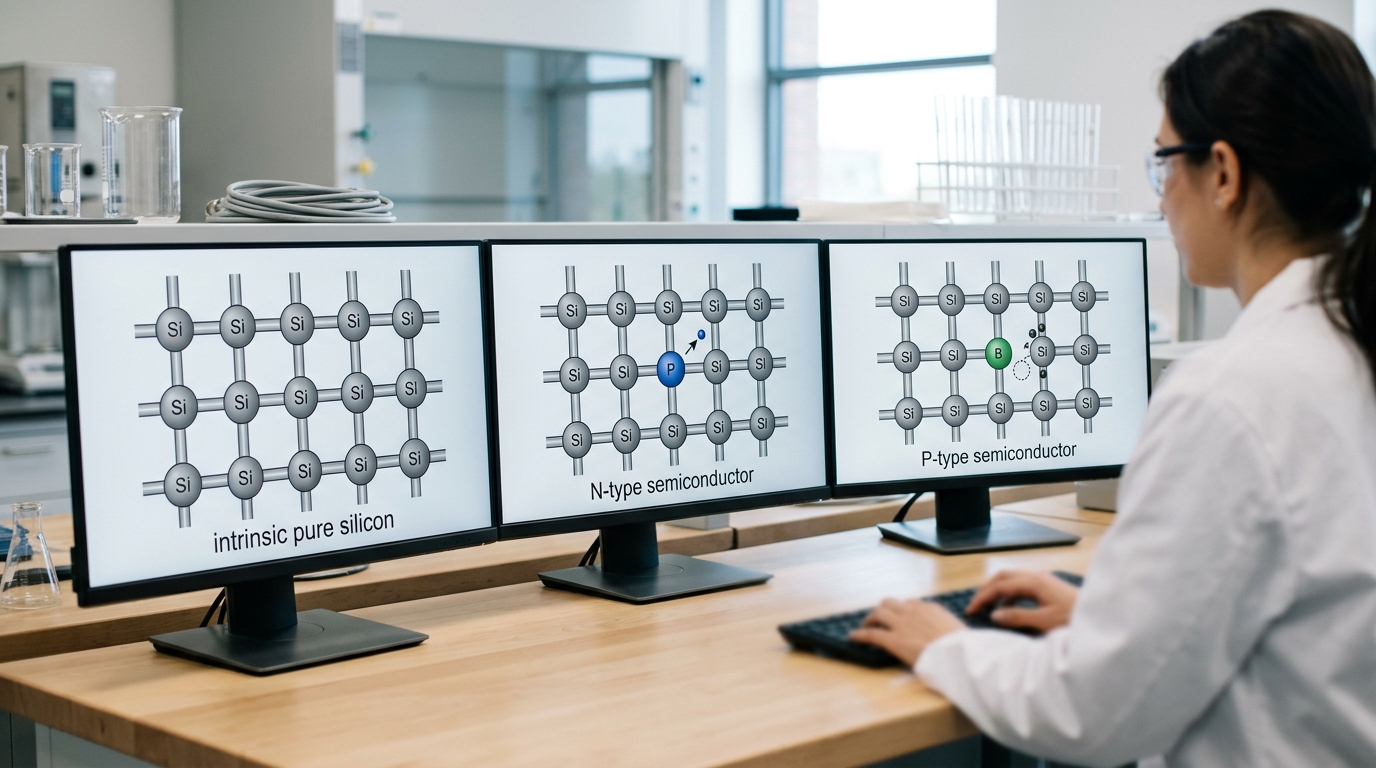
Intrinsic silicon is a clean crystal where every atom shares four electrons with the atoms next to it. At room temperature, only a handful of electrons break free, so it conducts really poorly.
A solid crystal that sits between a conductor and an insulator is pretty much useless until you hand it some spare charge carriers.
And that is exactly what doping does. The amount of impurity added is shockingly small. Often it is just 1 dopant atom for every 100 million silicon atoms, or roughly 0.000001%. That tiny bit alone can boost conductivity by a factor of thousands.
- N-type: Add phosphorus, which has 5 outer electrons. Four of them bond with silicon, and the fifth one just roams free. These extra electrons are the negative carriers here. Phosphorus is the donor, since it donates electrons.
- P-type: Add boron, which has 3 outer electrons. It leaves one bond empty, and that creates what we call a “hole.” Holes basically act like positive charges drifting through the crystal. Boron is the acceptor.
So why does any of this matter for class-12 physics and real chips alike? Honestly, because a transistor is just N-type and P-type regions pressed together.
The junction between them blocks current going one way and lets it through the other. No doping, no junction.
And without a junction, you get no logic gate and no CPU.
Here is one practical trap that engineers keep an eye on. The dopant atoms have to sit on the silicon lattice sites, not in between them. A misplaced atom doesn’t add a usable carrier at all. Instead it scatters them and completely ruins the device.
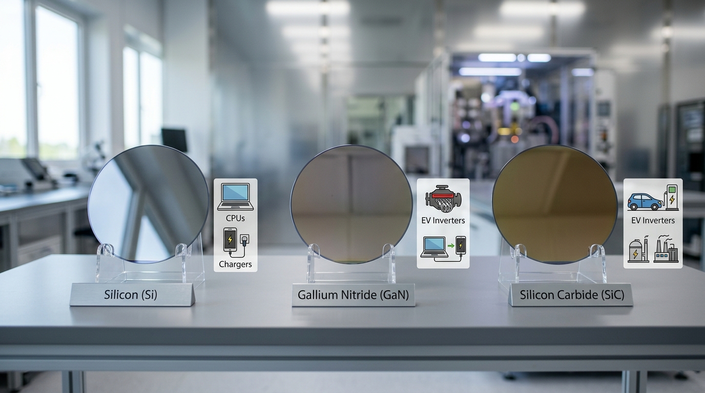
Silicon Versus GaN Versus SiC And Which Applications Each Material Enables
Pick the wrong material and you either waste money or melt your circuit. Silicon runs every logic chip on Earth.
Gallium nitride (GaN) makes phone chargers tiny. Silicon carbide (SiC) powers electric car inverters.
The split comes down to one number: band gap,the energy needed to push an electron into conducting mode.
Silicon has a band gap of 1.12 electron-volts. GaN sits at 3.4, and SiC at 3.26. Wider band gaps mean these wide-bandgap materials handle higher voltage and heat before failing. That single trait reshapes any honest analysis of what a semiconductor can do in power systems.
| Property | Silicon | GaN | SiC |
|---|---|---|---|
| Band gap (eV) | 1.12 | 3.4 | 3.26 |
| Breakdown field (MV/cm) | 0.3 | 3.3 | 3.0 |
| Switching speed | Moderate | Fastest | Fast |
| Max junction temp | ~approximately 150°C | ~approximately 200°C | ~approximately 200°C+ |
| Relative wafer cost | Lowest | High | Highest |
| Best use | Logic chips | Fast chargers, RF | EV inverters, grids |
Why not use GaN or SiC everywhere? Cost.
A SiC wafer runs several times pricier than silicon, so it only pays off where efficiency saves more. Tesla switched to SiC inverters in the Model 3, trimming power losses and extending range.
For power electronics in EVs and grids, that higher breakdown field is worth every dollar. Silicon still owns the billions of transistors inside your CPU,heat and voltage there stay low.
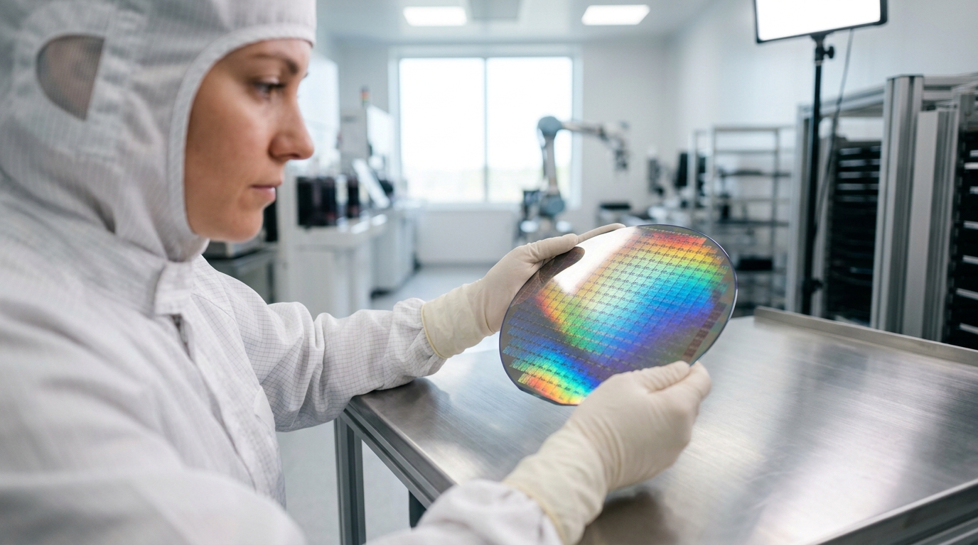
From Sand To Wafer How A Chip Is Actually Manufactured
A chip starts out as ordinary beach sand and ends up as a die that holds tens of billions of transistors on a fingernail-sized piece of silicon. That whole journey takes more than 1,000 separate process steps. Roughly three months go by for every wafer.
Any honest look at what is semiconductor and its application analysis really has to follow this physical chain. Why? Because the limits of how you build these things end up shaping what every product made from them can actually do.
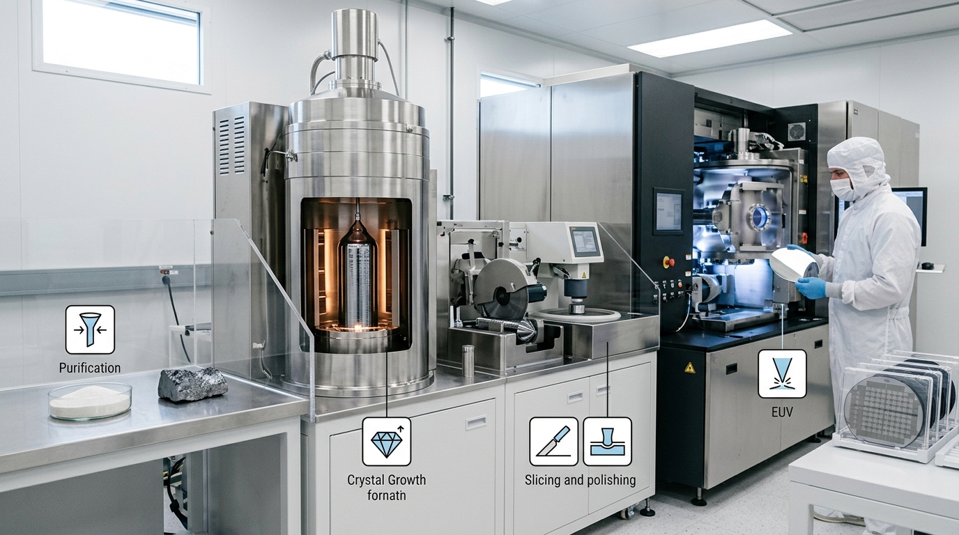
It all begins with quartz sand, which is mostly silicon dioxide. Furnaces heat that sand past approximately 1,700°C along with carbon to pull out the oxygen. What comes out is metallurgical silicon at approximately 98% purity, and honestly that is nowhere near clean enough.
So chipmakers refine it further to what people call “nine nines” purity, which is approximately 99.9999999%. They use the Siemens process to make polysilicon.
The rules are strict here. Fewer than one foreign atom is allowed per billion silicon atoms, because a single stray copper atom can completely ruin a transistor.
Next comes Czochralski crystal growth. A tiny seed crystal gets dipped into molten silicon, then slowly pulled upward while it spins, gradually drawing out one big cylindrical crystal we call an ingot. These ingots can reach approximately 300mm across and weigh over 100kg.
After that, a diamond wire saw cuts the ingot into wafers thinner than a credit card. Each wafer is then polished until it is mirror-flat, with variation down to just a few nanometers.
The pricey part is photolithography, which basically means printing circuit patterns using light. The most advanced nodes at 3nm and 5nm rely on extreme ultraviolet (EUV) machines from ASML. Each one of those costs over $150 million.
Light passes through a mask, the pattern shrinks down, and it exposes a light-sensitive coating. Then etching carves away the exposed silicon. Doping adds the impurities that turn that material into working transistors.
And this repeats, layer after layer, sometimes as many as 100 times.
So why does a single fab line cost over $20 billion? Consider TSMC’s Arizona facility on its own. It carries a price tag of roughly $40 billion.
EUV tools push that bill up. So do cleanrooms that are cleaner than a hospital surgery room, plus ultra-pure chemical systems. Finally, packaging seals the die and connects it to the outside world. That is the step that turns bare silicon into a chip you can actually use.
The next section breaks down the diodes, transistors, and integrated circuits that these wafers eventually become.
Core Semiconductor Devices Diodes Transistors And Integrated Circuits
So there are basically three building blocks that take silicon with stuff added to it and turn it into electronics that actually work. There’s the diode, the transistor, and the integrated circuit.
A diode works kind of like a one-way valve, but for electricity, letting current go through in only one direction.
A transistor acts like either a switch or something that boosts a signal. And an integrated circuit crams billions of those tiny switches onto one little chip.
Really, understanding any analysis of what a semiconductor is and its application starts with getting your head around these three devices first.
A PN-junction diode forms at the spot where p-type silicon, which has extra “holes,” meets up with n-type silicon, which has extra electrons. If you apply voltage one way, the current flows through easily.
But flip it around the other way, and the current just stops. This is what people call rectification, which basically means turning alternating current (AC) into direct current (DC).
And honestly, every phone charger you own depends on this happening.
Transistors really do most of the actual work here. A MOSFET (metal-oxide-semiconductor field-effect transistor) uses a bit of voltage on its gate to either open or close a channel sitting between two terminals. There are no moving parts at all, just an electric field doing the work.
A BJT (bipolar junction transistor) uses a small current to control a much bigger one, which is what makes it really good at boosting weak signals. MOSFETs generally rule digital chips, mostly because they sip almost no current when they’re just sitting idle.
Now, stack billions of those MOSFETs together and what you get is an integrated circuit. Apple’s M-series chips and Intel’s processors for data centers now hold tens of billions of transistors on a die smaller than a fingernail, all built at these tiny single-digit nanometer sizes.
Here’s a practical bit from the world of chip design, though. A transistor that leaks current when it’s supposed to be “off” wastes battery and gives off heat, and that’s exactly why modern chip factories worry so much about gate insulation.
These core semiconductor devices sit inside basically every CPU, memory chip, and microcontroller you own.
Inside One Smartphone The Dozens Of Distinct Chips Working Together
A single smartphone packs more than a dozen distinct semiconductor chips, each built from different materials and process nodes. The main processor handles logic.
⚠️ Common mistake: Assuming a “purer” silicon crystal makes a better semiconductor. This happens because people equate purity with performance, but undoped silicon barely conducts at all. The fix: deliberately add impurities—doping silicon with boron (P-type) or phosphorus (N-type) at parts-per-million levels is what creates the controllable current that makes transistors and the entire approximately $627 billion chip industry possible.
Memory chips store data. Separate chips manage power, radio signals, cameras, and charging.
No single chip does everything,and that division is the whole point of this part of any semiconductor and its application analysis.
Start with the brain. The SoC (system-on-chip),Apple’s A18 or Qualcomm’s Snapdragon 8 Elite,crams the CPU, GPU, and a neural engine onto one die built at a 3-nanometer node. It holds tens of billions of transistors on a piece of silicon smaller than your thumbnail.
Around it sit specialized partners:
- NAND flash — non-volatile storage that keeps your photos when the power is off. Built in stacked 3D layers, often 200+ tiers tall.
- DRAM — fast working memory the SoC reads from while apps run. It forgets everything the instant power drops.
- PMIC (power-management IC) — splits one battery voltage into the many voltages each chip needs.
- RF transceiver — converts digital data into the radio waves your 5G antenna sends.
- CMOS image sensor — turns light into pixels. Sony alone supplies sensors for a large share of premium phones, and CMOS technology dominates the digital camera market.
- GaN charger IC — uses gallium nitride, not silicon, to charge faster while staying cool.
Here is the practical insight: the RF section and the GaN charger often use compound semiconductors like gallium arsenide for high-speed signals, while logic and memory stay on silicon. One device, several material systems,because no single material wins at everything.
Where Semiconductors Are Used Across Computing Power Communications And Sensing
Four domains absorb most of the world’s chips: computing, power conversion, communications, and sensing. Each leans on a specific device and material from the chain we built earlier.
A data-center GPU runs on silicon transistors. An EV inverter runs on silicon carbide.
A 5G radio runs on gallium arsenide. A LiDAR sensor runs on a laser diode.
This is what an honest semiconductor and its application analysis looks like in practice.
Computing power: silicon CPUs and GPUs
NVIDIA’s H100 GPU packs roughly 80 billion silicon transistors built on a 4nm process node. Stack thousands of these in a training cluster and you get the engines behind modern AI models.
These are the same single-digit nanometer dies we traced from sand to wafer,just arranged for massively parallel math instead of general logic.
Power: SiC inverters in electric vehicles
The traction inverter flips a battery’s DC into AC for the motor. Tesla switched its Model 3 to silicon carbide MOSFETs, cutting switching losses and extending range. SiC’s higher breakdown field and thermal stability let inverters run hotter and smaller than silicon ever could.
Communications and sensing
- 5G RF chips: base-station power amplifiers use gallium arsenide and gallium nitride to push signals at approximately 28GHz cleanly.
- Automotive LiDAR: indium phosphide laser diodes fire pulses; silicon photodetectors time the bounce-back to map distance.
A 2025-model car may carry over 1,000 chips, per the Semiconductor Industry Association,spanning all four domains in one vehicle.
Emerging Applications AI Accelerators Quantum And Neuromorphic Chips
Three frontier chip types are pushing semiconductors past classic computing: AI accelerators, quantum processors, and neuromorphic chips. Each rewrites a different rule.
AI accelerators stack memory next to logic. Quantum chips trade transistors for qubits.
Neuromorphic chips copy how brain neurons fire. Any honest semiconductor application analysis must also name their real limits,cooling, error rates, and cost.
AI accelerators and HBM stacking
Modern AI training chips like NVIDIA’s H100 pair logic with High Bandwidth Memory (HBM),stacks of DRAM chips bonded directly above the processor to cut data travel distance. This matters because feeding data to the cores, not the math itself, is the bottleneck.
HBM3E delivers over 1 terabyte per second of bandwidth per stack, several times what older GDDR memory offered. The catch: stacking generates heat in a tiny space, so these packages need aggressive liquid cooling in data centers.
Quantum and neuromorphic chips
Quantum qubits come in two main flavors: superconducting loops (used by IBM) and silicon spin qubits. Both need cryogenic cooling near 15 millikelvin,colder than deep space.
Error rates remain the wall; a single qubit can flip from stray heat, so hundreds of physical qubits may be needed to build one reliable logical qubit.
Neuromorphic chips like Intel’s Loihi take a different path, mimicking how neurons spike to slash power use for pattern tasks, though software tools stay immature.
The Economic Weight Of Semiconductors And Common Misconceptions
Semiconductors are a worldwide business worth more than $600 billion a year, with revenue topping approximately $520 billion in 2023 and climbing since, according to Statista market data.
Yet two stubborn myths cloud how people understand this industry: that more transistors always mean faster chips, and that silicon is about to be replaced.
Both are wrong.
The money sits in very few hands. A handful of foundries produce most leading-edge chips, and a single Dutch company, ASML, builds every extreme ultraviolet lithography machine used to print the smallest features.
One of those machines costs over $150 million. That concentration is why a factory fire or an earthquake in one region can stall car production on the other side of the planet.
Myth 1: More Transistors Equal More Speed
Cramming more transistors onto a die raises capacity, not raw clock speed. Speed depends on architecture, memory bandwidth, and heat.
A chip with 50 billion transistors can run slower on your task than one with 20 billion if the software can’t use all those cores. Packing density helps parallel jobs like AI training, but a single-threaded program sees little gain.
Myth 2: Silicon Is Almost Obsolete
Silicon still forms the majority of integrated circuits manufactured worldwide. Materials like SiC and GaN win in power and high-frequency niches, but they cost more and lack silicon’s mature supply chain.
A serious study of what’s a semiconductor and its application analysis shows silicon staying dominant through the 2030s, not vanishing.
Practical tip: when a vendor quotes “billions of transistors” as a selling point, ask for benchmark numbers on your actual workload instead.
Frequently Asked Questions About Semiconductors And Their Uses
Short answers to the questions people actually search when they want a real-world semiconductor and its application analysis. No fluff, just the facts you need.
What are ten everyday examples of semiconductors?
Look around your home and you touch dozens of them daily:
- Smartphone processor — runs apps and the screen
- LED light bulb — the diode that glows
- Laptop SSD — flash memory storing your files
- Microwave control board — a microcontroller times the cooking
- Car key fob — a tiny radio-frequency chip
- USB charger — power transistors convert voltage
- Digital camera — a CMOS image sensor captures light
- Wi-Fi router — RF chips move data through the air
- Smart thermostat — temperature sensor plus a processor
- TV remote — an infrared LED sends the signal
What’s the difference between a semiconductor and a chip?
A semiconductor is the material, usually silicon. A chip is the finished product built from that material.
Think of it like flour versus a cake. One semiconductor wafer gets cut into hundreds of chips, each holding billions of transistors.
So every chip is made of semiconductor, but the words aren’t interchangeable.
Why does silicon dominate the industry?
Silicon stays the top choice for the majority of integrated circuits worldwide, per Britannica. Three reasons: it’s the second most abundant element in Earth’s crust, it forms a stable native oxide that works as a built-in insulator, and decades of tooling are optimized for it.
Switching materials means rebuilding fabs that cost over $20 billion each.
What materials may follow silicon?
Wide bandgap materials like silicon carbide (SiC) and gallium nitride (GaN) already win in electric-vehicle power systems. For logic chips, researchers eye gallium arsenide for speed and two-dimensional materials such as molybdenum disulfide for atom-thin transistors.
None replace silicon outright yet, they fill gaps where silicon hits physical limits.
Key Takeaways On What Semiconductors Are And Where They Matter
A semiconductor is a crystalline material whose conductivity sits between a metal wire and a glass insulator. That single property, controlled by doping and shaped by fabrication, turns ordinary sand into the brains of nearly every electronic device you own.
This is the heart of any honest analysis of what a semiconductor is and its applications.
The chain is simpler than it sounds. Silica sand becomes ultra-pure silicon.
The silicon becomes a wafer holding tens of billions of transistors on a fingernail-sized die, as Intel documents at single-digit nanometer nodes. Those transistors form diodes, logic gates, and integrated circuits.
The chips then land inside your phone, car, and laptop.
Material choice maps directly to the job:
- Silicon — logic, memory, and microcontrollers; the default for most chips.
- Silicon carbide (SiC) — EV inverters and grid power, where heat tolerance matters.
- Gallium nitride (GaN) — fast chargers and RF, prized for speed and efficiency.
- Gallium arsenide (GaAs) — lasers and optical links in fiber and 5G.
Why does this matter beyond engineering? A market that topped approximately $520 billion in 2023 sits behind the screens, sensors, and networks that run daily life. Pull semiconductors out, and modern healthcare, banking, and transport stop.
Want to go deeper? Skip the textbooks first. Read a real device datasheet, pick an MOSFET (a power-switching transistor) and study its breakdown voltage and thermal ratings. Then compare a silicon part against a SiC equivalent. That side-by-side teaches material selection faster than any summary.


