
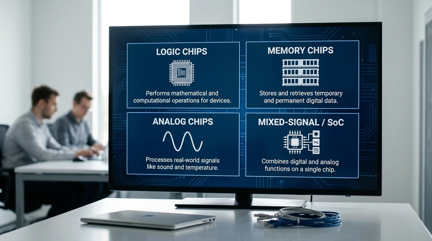
The four main types of semiconductor chips are logic, memory, analog, and “other” devices (covering discrete and optoelectronic parts), according to the OECD’s 2024 semiconductor taxonomy. Logic chips handle calculations, memory chips store data, analog chips process real-world signals like sound and light, and the “other” category manages power, lighting, and sensing. Most modern devices use all four together. With the global chip market projected to reach roughly $697[1] billion in 2026, each category claims a significant share of total demand.
Logic chips do the thinking, memory chips store data, analog chips translate real-world signals like sound and light, and the “other” group handles power, lighting, and sensing.
So which type powers your phone, your car, or the AI server running your favorite chatbot? Usually all four work together.
The global chip market is projected to reach roughly $697[2] billion in 2026, and each of these four categories claims a real slice of that demand. Below, you’ll see exactly what each type does, where it shows up, and why the line between them keeps blurring.
Quick Takeaways
- Logic chips handle calculations and decisions, powering processors in phones and computers.
- Memory chips store and retrieve data; analog chips process real-world signals.
- The OECD’s 2024 taxonomy sorts chips into logic, memory, analog, and “other” categories.
- Mixed-signal and SoC designs combine multiple chip functions on one silicon piece.
- Global chip market projected to hit roughly $697[3] billion in 2026.
The 4 Main Types of Semiconductor Chips at a Glance
The four main types of semiconductor chips are logic chips, memory chips, analog chips, and mixed-signal/SoC chips. Logic chips run calculations and make decisions.
Memory chips store and retrieve data. Analog chips handle real-world signals like sound, heat, and light.
Mixed-signal chips and system-on-chip (SoC) designs combine these jobs on one piece of silicon.
This grouping isn’t just a textbook idea. The OECD’s 2024 semiconductor taxonomy sorts chips into four functional buckets: logic, memory, analog, and a catch-all “other” group covering discrete and optoelectronic parts.
ASML uses a similar split, listing logic, memory, application-specific integrated circuits (ASICs, chips built for one fixed task), and SoCs.
Here’s the quick-reference version. Use it to spot which category any chip falls into:
| Chip Type | Core Job | Common Examples |
|---|---|---|
| Logic | Process data, run instructions | CPU, GPU, microcontroller (MCU) |
| Memory | Store and recall data | DRAM, NAND flash, SRAM |
| Analog | Manage continuous physical signals | power management ICs, RF transceivers, sensors |
| Mixed-signal / SoC | Blend analog + digital on one die | smartphone chips, audio codecs |
One thing trips up beginners: these categories overlap in real products. A modern phone processor is technically an SoC, yet it packs logic cores, memory blocks, and analog radios inside.
Knowing the four base types of semiconductor chips first makes those hybrids far easier to read on a spec sheet.
Logic Chips and What They Compute
Logic chips are the decision-makers. They take in instructions, run the math, and tell the rest of a device exactly what to do next.
Out of the four types of semiconductor chips, logic chips handle every “if this, then that” choice, from opening an app to drawing a single frame of video.
IMEC describes them as chips built for processing and making decisions, which is basically the opposite of memory chips that just hold onto data.
So what actually sets a logic chip apart from the others? It comes down to two things.
How many transistors it packs and how many instructions it can push through. A transistor is really just a tiny switch flipping between 0 and 1.
Cram in more switches, and the chip can take on more work at the same time.
Take the NVIDIA H100 GPU, which was built for training AI. It holds roughly 80 billion transistors. A regular CPU like the Intel Core or AMD Ryzen does things differently, though. It spreads everyday tasks across several cores, and each core handles its own stream of instructions.
The Main Logic Chip Families
- CPU (microprocessor): This is the all-purpose brain. It runs your operating system and most of your software. Intel Core and AMD Ryzen pretty much rule desktops and laptops.
- GPU: This one is built to do thousands of small math operations all at once. That makes it great for graphics and AI. The H100 honestly became the go-to chip for 2025 data-center AI builds.
- ASIC: An application-specific integrated circuit is a chip designed for one job and one job only, like mining Bitcoin or decoding video. There is no wasted circuitry inside it.
Here is something engineers tend to learn the hard way. A GPU isn’t always faster than a CPU. For tasks loaded with branching logic, meaning lots of decision points, a CPU often comes out ahead. That’s because GPUs really struggle with code that keeps changing direction on them.
Match the chip to the actual workload, not to the hype.
Memory Chips and How They Store Data
Memory chips store data so other chips can use it. Among the four types of semiconductor chips, memory splits into two families: volatile and non-volatile.
Volatile memory loses everything when power cuts off. Non-volatile memory keeps data even after shutdown.
That single difference decides where each chip belongs in a device.
DRAM (dynamic random-access memory) is the workhorse of volatile storage. It holds each bit in a tiny capacitor that leaks charge, so it must refresh thousands of times per second.
Samsung’s DDR5 modules run far faster than older DDR4 and feed data into CPUs without stalling them. SRAM (static RAM) is the speedy cousin, it uses six transistors per bit, needs no refresh, and lives inside processor caches.
Because SRAM costs more per gigabyte, chips use it only in small amounts.
Non-volatile flash splits into two designs. NAND flash packs cells densely and powers SSDs, phones, and USB drives. NOR flash reads faster and stores boot code in cars and routers. Wikipedia’s flash memory overview explains the wiring difference clearly.
Why Memory Bandwidth Bottlenecks AI Training
AI accelerators starve without fast memory. Training a large model means moving billions of parameters between memory and compute cores every second.
SK Hynix HBM3 (high-bandwidth memory) stacks DRAM dies vertically and connects them with thousands of through-silicon vias, hitting bandwidth far above standard DDR5. NVIDIA’s H100 GPUs pair with HBM3 for exactly this reason.
A practical tip from chip design work: profile your workload before buying memory. If your model is bandwidth-bound, faster HBM helps more than extra compute cores.

Analog Chips and Why They Handle the Physical World
Analog chips deal with continuous signals, which are the smooth, always-shifting voltages that come from sound, light, heat, and radio waves. Among the four types of semiconductor chips, analog is the one that actually talks to the physical world around us.
You can’t fully swap it out for digital. Why? Because the real world doesn’t run on clean 0s and 1s.
Picture a microphone for a second. Your voice makes a wave that rises and falls in countless tiny steps.
A digital chip only knows fixed values. An analog chip grabs that wave first, then passes it along.
IMEC explains that analog chips work with continuous signals, while digital chips deal with binary ones instead.
Where Analog Chips Live
- Power management ICs (PMICs) — these control voltage so that a battery’s messy output turns into a steady, reliable supply. Texas Instruments’ TPS series shows up across phones and cars.
- RF chips — these manage radio waves for Wi-Fi, cellular, and GPS signals.
- Sensors — these turn temperature, pressure, or motion into electrical signals you can use.
- Audio amplifiers — these take weak audio signals and boost them strong enough to drive speakers and headphones.
Analog Devices makes high-precision parts. Things like its ADAU audio codecs and AD-series data converters, which essentially bridge the analog and digital worlds together.
Why Digital Can’t Take Over
In electric vehicles, an inverter has to control motor current that swings thousands of times every second. That really calls for analog and power chips built on materials like silicon carbide.
IBM notes that doped materials such as GaN and GaAs are the foundation for these RF and power devices.
5G radios run into the same wall. Their antennas pick up faint analog waves measured in microvolts.
No digital logic can read a signal that doesn’t even exist in digital form yet. So the analog front end has to amplify and clean it up first. Skip the analog part, and honestly the physical world never reaches your processor at all.
Mixed-Signal Chips and System-on-Chip Designs
A mixed-signal chip puts analog and digital circuits on one piece of silicon, called a die. A system-on-chip (SoC) goes further, it packs logic, memory, and analog functions onto that single die.
This is why your phone runs on one main chip instead of dozens. ASML lists SoC devices as one of four main microchip categories by functionality.
The mix happens because real signals are messy. A radio antenna picks up an analog wave.
A converter (ADC, short for analog-to-digital converter) turns it into 0s and 1s. The digital logic then processes those bits.
Building both on one die avoids the speed loss and noise you get when signals jump between separate chips.
Apple’s A-series and M-series prove the point. The Apple M-series chip combines the CPU, GPU, neural engine, and memory controller in one package. Qualcomm’s Snapdragon SoCs do the same for Android phones, folding in a modem, image processor, and AI accelerator.
Why Phones Consolidated Dozens of Chips Into One
Early smartphones used separate chips for the processor, modem, audio, and power. That ate board space, drained batteries, and raised cost. Squeezing them onto one SoC cut all three.
- Space: A modern SoC fits in a few square millimeters, freeing room for a bigger battery.
- Power: Shorter internal wires mean less energy lost moving data.
- Cost: One die is cheaper to make and test than many.
One practical catch designers face: analog blocks are sensitive to digital noise. Place a fast clock line too close to an analog converter, and you get errors. That’s why mixed-signal layout among the types of semiconductor chips is some of the hardest engineering work in the field.
Chip Type Comparison by Performance, Power, and Cost
Logic chips win on raw speed but burn the most power and cost the most to build. Memory chips trade speed for storage density.
Analog chips sip power and stay cheap because they don’t need the newest factories. SoC designs balance all three, at the price of complex engineering.
The table below shows how the four types of semiconductor chips stack up.
| Chip Type | Processing Speed | Power Draw | Typical Fab Node | Relative Wafer Cost |
|---|---|---|---|---|
| Logic (CPU/GPU) | Fastest — billions of operations per second | High (5–approximately 250W[4]) | 3nm–7nm | Highest |
| Memory (DRAM/NAND) | Moderate — bound by access latency | Medium (2–approximately 15W[5]) | 10nm–14nm class | High |
| Analog | Low — measured in MHz, not GHz | Very low (milliwatts) | 28nm–180nm | Low |
| SoC / Mixed-Signal | High on digital blocks, modest on analog | Variable (1–approximately 15W[6]) | 3nm–16nm mix | Medium–High |
The node gap drives most of the cost. A “node” measures the smallest feature a factory can print, smaller means faster and denser.
A 3nm wafer runs roughly $20,000[7], while a mature 28nm wafer costs near $3,000[8], according to industry pricing data tracked by the Semiconductor Industry Association. That nearly 7x gap is why analog chips stay on older nodes, shrinking them adds cost without helping signal quality.
The pitfall I see teams make follows directly from that gap: chasing 3nm for an analog or power chip. It wastes money. Match the node to the job, reserve nodes for logic and SoC blocks that genuinely need the speed.
Which Chip Types Power Smartphones, EVs, Data Centers, and AI
Match the device to the chip: smartphones run on SoCs, electric vehicles lean on power analog and microcontrollers, data centers stack GPUs with high-bandwidth memory, and AI training pushes that same GPU-plus-HBM combo to its limit.
Knowing which of the four types of semiconductor chips dominates each product tells you where the real engineering, and the real money, goes.
Smartphones — the SoC does almost everything
A modern phone packs a system-on-chip (SoC) that fuses CPU cores, a GPU, an image processor, and a modem onto one die. Apple’s A18 and Qualcomm’s Snapdragon lines are the textbook examples.
ASML notes that SoC and ASIC designs sit alongside standalone logic and memory as the main chip categories, and phones favor SoCs to save space and battery.
Around the SoC sit analog and power-management ICs (PMICs) that regulate voltage to every component. One pitfall buyers miss: the camera “magic” is mostly the ISP block inside the SoC, not the lens.
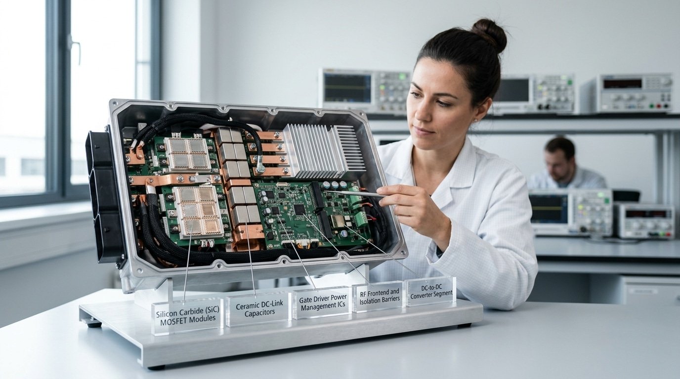
Electric vehicles — power analog rules
An EV is a moving power-electronics lab. Silicon carbide (SiC) inverters convert battery DC into motor AC, while dozens of microcontrollers (MCUs) run brakes, steering, and battery management. A single car can carry 1,000,3,000 chips.
- SiC power chips — handle approximately 800V[9] battery systems with less heat loss
- MCUs — control discrete subsystems like airbags and climate
- Analog sensors — track current, temperature, and tire pressure
Data centers and AI training — GPUs plus HBM
AI workloads stack logic and memory together. Nvidia’s H100 and GB200 pair thousands of GPU cores with High-Bandwidth Memory (HBM), stacked memory that sits beside the processor to cut data-fetch delay.
SK hynix reported that HBM demand surged with AI servers, making it one of the fastest-growing memory segments through 2025.
Practical tip: for AI training, memory bandwidth, not raw core count, is usually the bottleneck. That’s why HBM placement matters more than buyers expect.
Emerging Chip Types — NPUs, TPUs, RISC-V, and Chiplets
Beyond the four classic types of semiconductor chips, a new wave of specialized designs now drives AI and modern computing. The big four: NPUs for on-device AI, Google’s TPUs for cloud training, the open RISC-V instruction set, and chiplet-based packaging.
These aren’t replacing logic or memory, they reshape how those chips get built and used.
NPUs and TPUs: chips built only for AI math
A neural processing unit (NPU) is a logic chip tuned for one job, running the matrix math behind AI models. Phone SoCs from Apple, Qualcomm, and MediaTek now ship NPUs that handle photo processing and voice commands without sending data to the cloud.
That keeps your face-blur and live translation running fully offline.
Google’s Tensor Processing Unit (TPU) is the data-center cousin. It’s an ASIC, a chip wired for a fixed task, designed to train massive AI models. Google’s Cloud TPU documentation shows these run training jobs that would choke a general-purpose CPU.
RISC-V: the open-source instruction set
RISC-V isn’t a chip, it’s a free instruction set (the rulebook a processor follows). Unlike Arm or x86, anyone can build a RISC-V core without paying license fees.
According to RISC-V International, the standard now has thousands of member organizations worldwide. That cuts cost for startups and lets countries design home-grown chips.
Why chiplets beat one giant die
Here’s the cost problem: a single large die (one piece of silicon) fails more often during manufacturing. One flaw kills the whole chip. Chiplets split a processor into smaller pieces, then stitch them together in one package.
AMD’s Ryzen and EPYC chips pioneered this, small 7nm compute chiplets paired with a cheaper I/O die. Intel’s Foveros stacks chiplets vertically.
The payoff is yield: smaller dies have fewer defects per wafer, so more usable chips per batch. That math is why monolithic designs are fading at the high end.
Frequently Asked Questions About Semiconductor Chip Types
Quick answers to the questions people ask most about chip categories, makers, and materials.
Is Apple an IDM or fabless company?
Apple is fabless. It designs its own chips, like the M-series and A-series SoCs, but never builds them.
The actual manufacturing happens at TSMC’s foundries in Taiwan. An IDM (integrated device manufacturer) such as Intel both designs and fabricates its chips in-house.
Apple skips the factory step, which is why it depends on TSMC’s 3nm process for its newest silicon.
How many types of semiconductor chips are there?
It depends on who’s counting. The OECD’s 2024 semiconductor taxonomy lists four main functional types: logic, memory, analog, and an “other” group covering discrete and optoelectronic devices.
ASML uses a slightly different four-bucket model, logic, memory, ASICs, and SoCs. The four classic types of semiconductor chips covered in this guide line up with the OECD framework.
What metal are chips made from?
Chips aren’t made from a single metal. The base is silicon, a semiconductor element, not a metal.
On top of that, makers add thin layers of copper for wiring, aluminum for older connections, and trace amounts of materials like tungsten. Copper replaced aluminum in most logic chips because it conducts electricity with less resistance, letting signals move faster.
What are computer chips used for?
Computer chips do three core jobs: compute, store, and connect. A CPU runs instructions. DRAM holds active data. Analog chips manage power and signals. Together these types of semiconductor chips run everything from your laptop to data center servers.
Choosing the Right Chip Type for Your Application
Start with your hardest constraint, then pick the chip. If raw compute speed rules your design, lead with a logic chip.
If you move and hold large data sets, budget for memory. If your product touches the real world, sound, light, temperature, analog and mixed-signal chips become non-negotiable.
The four classic types of semiconductor chips rarely live alone. A smart thermostat needs analog sensing, logic for decisions, and a small memory block to hold its schedule. So the real question is: which chip dominates your bill of materials and your power budget?
A Quick Decision Checklist
- Need to run code or AI models? Logic chip first — CPU, GPU, or NPU depending on workload type.
- Storing large data fast? DRAM for speed; NAND flash for cheap, persistent bulk storage.
- Reading physical signals? Analog front-end, often paired with a mixed-signal ADC.
- Tight space and cost limits? An SoC folds multiple functions onto one die.
- Shipping in millions of units? A custom ASIC lowers per-unit cost despite high upfront design fees.
The most common pitfall in product reviews ties back to that memory-versus-compute balance: teams over-spec the logic chip and starve the memory bandwidth. A fast processor that waits on slow DRAM wastes both money and power. Match memory speed to compute demand before you finalize the board.
Cost scale matters too. The global semiconductor market is forecast to reach roughly $1[10] trillion in annual sales by 2030, which means chip prices for niche designs stay high until volume catches up.
Investors should track which segment, logic, memory, or analog, drives a company’s margin, since each behaves differently across the cycle.
Map your top constraint to its chip category. Get that match right, and the rest of your design falls into place.


