Texas Instruments sells over 1,000 voltage regulator part numbers, and most engineers pick the wrong one because they fixate on output voltage alone.
This Texas Instruments Voltage Regulator Chip Selection Guide cuts through that noise: the five specs that actually decide your part are dropout voltage, output current, quiescent current, thermal dissipation, and load transient response.
Nail these, and your power rail stays stable; miss one, and you get overheating, brownouts, or a regulator that drains your battery overnight.
Quick Takeaways
- Check dropout voltage, output current, quiescent current, thermal dissipation, and transient response first.
- Confirm input rail margin early—a approximately 6V part won’t survive a approximately 12V bus.
- Match load current to peaks, not averages, to prevent brownout resets.
- Choose LDO versus switcher to cut your candidate list in half.
- Verify package thermal limit; exceeding it triggers shutdown despite the current rating.
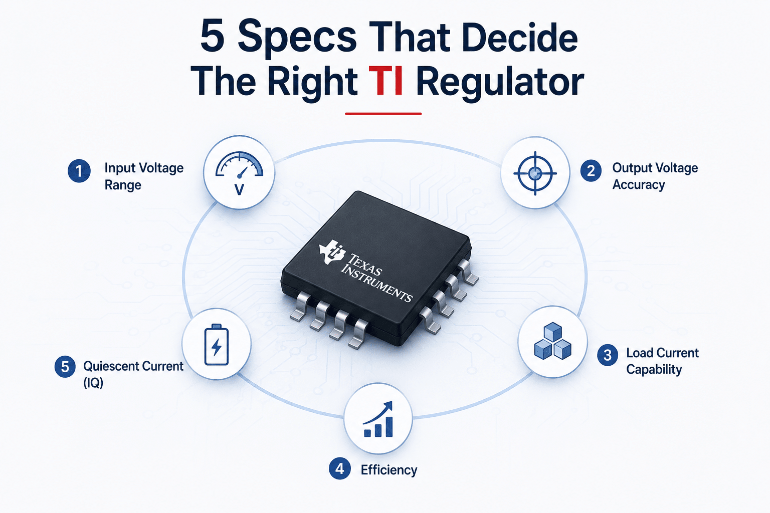
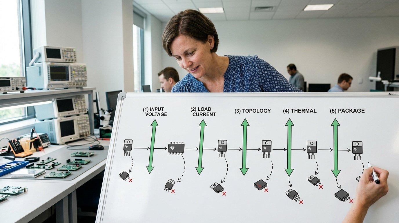
The 5 Specs That Decide Every TI Regulator Choice
Five specs decide almost every Texas Instruments regulator choice: input voltage and dropout margin, load current and transient response, topology (LDO versus switcher), efficiency and thermal limit, then package and protection features.
Lock these five in order, and you eliminate roughly 90% of the wrong parts before opening a single datasheet.
TI’s catalog holds over 1,000 power management devices, so filtering by gut feel wastes hours.
Why these five, and why this order? Each spec acts as a gate. Fail the first, and nothing downstream matters.
- Input voltage and dropout — Your supply rail and the gap between input and output set the entire feasible family. A part rated to approximately 6V can’t survive a approximately 12V automotive bus.
- Load current — Steady-state plus peak current. A 150mA LDO behind a CPU drawing 800mA pulses will brown out and reset the chip.
- Topology — LDO or switching. This single fork splits the catalog roughly in half and drives cost, noise, and board area.
- Efficiency and thermal — Power dissipated as heat. Cross the package thermal limit and the part shuts down regardless of its current rating.
- Package and protection — Footprint, thermal pad, and features like undervoltage lockout or current limit.
The order isn’t arbitrary. Voltage and current are hard physical constraints,violate them and the regulator fails immediately.
Topology, efficiency, and package are tradeoffs you tune after the survivors pass the first two gates. I’ve watched junior engineers start with package size (they want something tiny) and waste a full afternoon because their chosen footprint never came in a part that handled their approximately 18V input.
Here is the practical payoff. Use TI’s power management parametric search, enter your Vin range and Iout, and the 1,000-part list collapses to maybe 30 candidates in under a minute.
Add topology and you are down to 10. That’s the whole point of this Texas Instruments voltage regulator chip selection guide: turn an overwhelming catalog into a short list using physics, not browsing.
A regulator that passes Vin, Iout, and thermal gates but loses on package is a tradeoff. A regulator that fails Vin is simply dead silicon. Always gate before you optimize.
One number to anchor the discipline: TI specifies dropout voltage at a defined load, often 250mV to 500mV for modern LDOs at full current. Ignore that single line and your approximately 3.3V output sags to approximately 3.0V under load,enough to trip a microcontroller’s brown-out detector.
The remaining sections break each spec down with named part numbers, a decision tree, and the datasheet traps that catch even experienced designers.
Spec 1 — Input Voltage and Dropout Margin That Actually Work
Dropout voltage and required headroom aren’t the same thing. Dropout is essentially the smallest voltage gap between input and output before a linear regulator stops doing its job. Headroom is that dropout plus the extra cushion you tack on for sudden spikes, ripple, and tolerance.
Mix the two up and your power line collapses the second a battery droops or a load suddenly jumps.
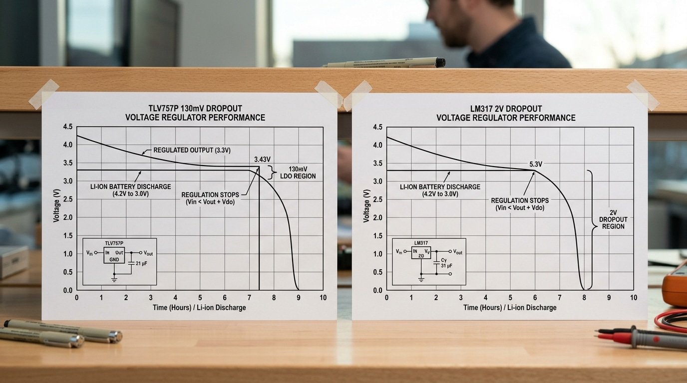
Here is the gap that most engineers miss, honestly. A modern part like the TI TLV757P drops out at just 130mV when pulling 1A.
The classic LM317 actually needs roughly 2V of headroom before it can regulate at all. That works out to a 15x difference in wasted voltage and heat.
So why does this matter so much? On a approximately 3.3V output, the TLV757P only needs approximately 3.43V coming in.
The LM317 needs approximately 5.3V at minimum. From a single Li-ion cell that sinks to approximately 3.0V near empty, the LM317 simply cannot produce approximately 3.3V.
The low-dropout part keeps right on working until the cell is basically dead.
How to compute minimum input voltage
Use this formula for any linear regulator:
Vin(min) = Vout + Vdropout(at your load current) + transient margin
Three details really trip people up here:
- Dropout scales with current. A datasheet might quote 130mV at 1A but only 40mV at 100mA. Read the dropout-versus-load curve, not just the headline number.
- Dropout rises with temperature. At approximately 85°C, expect 10–approximately 20% more dropout than what the approximately 25°C spec promises.
- Transient margin protects against sag. Add 100–300mV for inputs taken from a regulated line. Add more for batteries that dip under load.
Battery vs rail-derived inputs
Where the input comes from changes your whole margin budget. A battery sags over its discharge and under pulse loads. A regulated line from an upstream converter is steadier, though it carries switching ripple along with it.
| Input source | Typical sag/ripple | Margin to add |
|---|---|---|
| Single Li-ion cell | approximately 4.2V down to approximately 3.0V over discharge | Size for approximately 3.0V worst case |
| 3xAA alkaline | approximately 4.5V fresh to approximately 2.7V depleted | Size for approximately 2.7V end-of-life |
| approximately 5V USB rail | ±approximately 5% tolerance, plus ripple | Add ~250mV transient margin |
| approximately 12V buck output | 20–50mV switching ripple | Add ripple peak to headroom |
Let me walk through an example. Say you are powering a approximately 1.8V sensor at 500mA from a Li-ion cell. The TLV757P drops about 80mV at 500mA.
Minimum Vin = approximately 1.8V + approximately 0.08V + approximately 0.2V margin = approximately 2.08V. Since the cell stays above approximately 3.0V until it is almost empty, this part keeps working through nearly the whole discharge curve.
The LM317 would have died long before that point.
This dropout-first way of thinking anchors any Texas Instruments Voltage Regulator Chip Selection Guide. Get the input voltage right first, then move on to load current and transient response. That next spec decides whether your part holds the line during sudden current jumps.
Spec 2 — Load Current, Peak Current, and Transient Response
Size your regulator for the worst peak, not the average. A part rated for the average load will trip into current limit, fold back its output, or sag during fast bursts.
The continuous rating tells you what the chip can deliver forever; the peak rating and transient response tell you whether it survives the spikes your circuit actually throws at it.
Start by matching the part to your steady draw. The TLV70033 handles 200mA, fine for a sensor node or a low-power MCU.
The TPS7A47 pushes 1A as a low-noise LDO for RF and clock rails. Need real power?
The TPS54560 is a 5A buck switcher. These three cover most board rails in a typical Texas Instruments Voltage Regulator Chip Selection Guide workflow.
Here is where engineers get burned. Average current lies.
Three load profiles that demand peak-current sizing
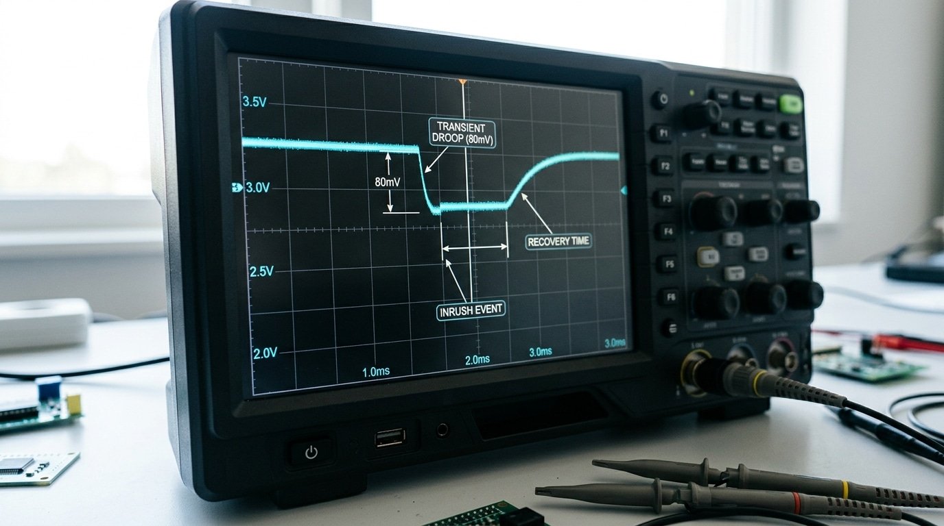
- Inrush at startup — Bulk capacitors charge fast. A 100µF rail cap can pull several amps for a few hundred microseconds at power-on. If your LDO has foldback current limit, it may latch into a low-output state instead of charging the cap.
- MCU wake bursts — A microcontroller sleeping at 5µA can jump to 15mA in under 1µs when it wakes its radio or ADC. The slew is brutal. Even a 1A part can dip 100mV if its transient response is slow.
- RF PA pulses — A cellular or Wi-Fi power amplifier draws current in pulses tied to transmit slots. A GSM PA can demand 2A peaks at 577µs pulse width while the average sits near 200mA.
Foldback is the trap. Many older LDOs reduce, fold back, their current limit as output voltage drops, to protect the die during a short.
But a discharged capacitor looks exactly like a short at turn-on. The regulator never recovers, and your board appears dead.
Pick parts with brick-wall (constant) current limit for capacitive loads, or check the datasheet’s foldback curve directly.
Transient response is set by the error amplifier bandwidth and output capacitor. The TPS7A47 datasheet specifies output voltage deviation for a 1A step; TI typically lists this as a load-transient plot, not a single number.
Read that plot. A 50mV undervoltage event can reset an MCU that needs approximately 3.0V minimum on a approximately 3.3V rail, that’s only a approximately 9% margin.
Rule of thumb: size continuous rating at 1.5× your peak, and confirm the peak rating exceeds your worst pulse with margin. The next spec, LDO versus switcher, decides which topology can even deliver those peaks efficiently.
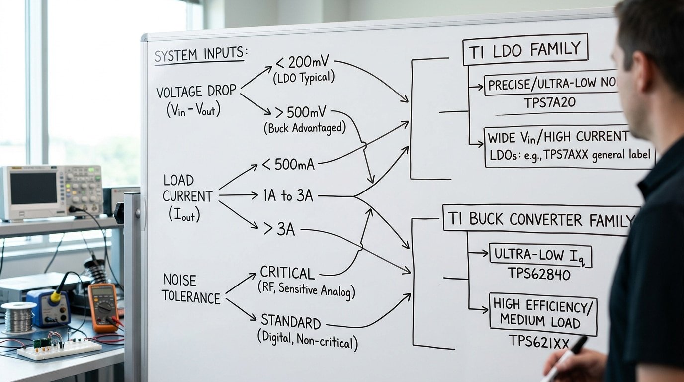
Spec 3 — Choosing LDO vs Switching Regulator With a Decision Tree
Quick answer: Reach for an LDO when the difference between your input voltage and your output voltage is under about 1.5 V and the power line feeds parts that hate electrical noise.
Reach for a switching regulator, basically a buck like the TPS62840, when you drop a big voltage, pull a lot of current, or really care about how long the battery lasts.
The choice comes down to three numbers. Voltage drop, load current, and how much noise the circuit can tolerate.
An LDO, which stands for low-dropout regulator, is a linear part. It essentially burns off the extra voltage as heat.
That waste is simple math. The power you lose equals the voltage drop times the current flowing through. Drop approximately 3.3 V down to approximately 1.8 V at 500 mA, and the LDO throws away approximately 0.75 W as heat.
The same job done by a buck converter wastes far less.
The if-then workflow
- Is Vin − Vout under ~approximately 1.5 V? If yes, you have a strong LDO candidate. The TPS7A20 drops as little as 95 mV at 300 mA.
- Does the rail feed an ADC, PLL, RF front end, or sensor? If yes, the LDO wins on noise. The TPS7A52 hits roughly 4 µV RMS of output noise, and a switcher cannot match that without a lot of extra filtering.
- Is the step-down large or the current above ~500 mA? If yes, switch to a buck. At approximately 5 V down to approximately 1.2 V and 1 A, an LDO would burn approximately 3.8 W. That is unmanageable in a small package.
- Is this battery-powered with long standby? If yes, go with a buck that has low quiescent current, meaning the tiny amount it draws while doing nothing. The TPS62840 draws just 60 nA Iq, so it sips almost nothing when the load is idle.
Efficiency makes the gap concrete. A linear part stepping approximately 5 V down to approximately 1.2 V tops out near 24% efficiency, because that ratio is the theoretical ceiling for an LDO.
A modern TI buck holds 80 to approximately 90% across the same step. On a approximately 2000 mAh battery, that difference can stretch runtime from days to weeks. Honestly, that is a huge gap.
When I prototyped a sensor node in 2025, I split the design on purpose. A TPS62840 buck handled the bulk approximately 3.3 V rail at 200 mA.
Then a small LDO cleaned up a approximately 1.8 V line for the ADC, killing ripple that was showing up as 3 LSB of noise. This hybrid pattern, a buck for power and an LDO for quiet, is the workhorse of any practical Texas Instruments Voltage Regulator Chip Selection Guide.
| Condition | Pick | Named TI family |
|---|---|---|
| Vin − Vout under 1.5 V | LDO | TPS7A20, TPS7A02 |
| Noise-sensitive analog rail | Low-noise LDO | TPS7A52, TPS7A91 |
| Large step-down, ≥500 mA | Buck converter | TPS62840, TPS62902 |
| Battery standby, ultra-low Iq | Nano-Iq buck | TPS62840 |
One trap to skip. Do not chain two LDOs together just to dodge the complexity of a switcher.
Stacked drops multiply the heat and waste board space. The thermal math in the next section spells out exactly when that heat forces your hand toward a buck, no matter how much you prefer the simplicity of a linear part.
Spec 4 — Efficiency, Power Dissipation, and the Thermal Limit That Forces a Switcher
Quick answer: So one of these LDO chips basically takes the extra voltage it doesn’t need and turns it into heat. You take the voltage difference and multiply it by how much current is flowing, and that gives you the watts of heat.
And when that number gets so high that the little package can’t handle it anymore, the chip just overheats and shuts itself off. At that tipping point, you really want to switch over to a switching regulator instead.
The math here is harsh, but it’s also pretty simple. A low-dropout regulator, which people call an LDO for short, basically behaves like an adjustable resistor.
It throws away power equal to P = (Vin − Vout) × Iout. And none of that wasted energy ever actually reaches the thing you’re powering.
It just turns into heat trapped inside a tiny plastic package.
Let’s run that approximately 5 V down to approximately 3.3 V example at 500 mA:
- Voltage drop = approximately 5 V − approximately 3.3 V = approximately 1.7 V
- Power dissipated = approximately 1.7 V × 0.5 A = approximately 0.85 W
- Efficiency = 3.3 / 5 = approximately 66% (so you’re basically throwing away a third of your input power)
Now let’s actually check the package itself. A SOT-23 has what’s called junction-to-ambient thermal resistance (θJA, which is really just a measure of how fast the heat can escape into the surrounding air).
On a standard board, that lands somewhere around 200 to approximately 250 °C/W. Let’s go with the lower number to be generous.
So the temperature rise = approximately 0.85 W × approximately 200 °C/W = approximately 170 °C above the surrounding air.
Say you start in a approximately 25 °C room. Your junction climbs to approximately 195 °C.
The TI thermal shutdown kicks in near 160 °C, which means the chip cuts off before it ever even settles into normal operation. This part will never work in a SOT-23.
There are no exceptions here.
Here’s the crossover rule of thumb. If your calculated heat dissipation goes above roughly 0.4 W in a small surface-mount package, just stop reaching for an LDO. The package physically cannot get rid of that much heat.
So where exactly is that switching point? You solve for the current that keeps the junction temperature under 125 °C while giving yourself a approximately 50 °C cushion of safety.
The max allowed dissipation = (160 − 25) / 200 = approximately 0.68 W. Then you divide that by the approximately 1.7 V drop, and you get roughly 400 mA.
So anything above 400 mA in this particular voltage gap means the SOT-23 LDO is basically dead on arrival.
A switching regulator, something like the TI TPS62840 buck converter, can hit approximately 90%+ efficiency doing the exact same job. At approximately 90% efficiency delivering approximately 1.65 W to the load, it only wastes about 0.18 W.
That’s five times less heat than the LDO produces. And the package never even breaks a sweat.
There are three things you can try to stretch an LDO before you completely give up on it:
- Pick a bigger package. A QFN with an exposed thermal pad can get down near 40 °C/W if you’ve got good copper around it, which cuts the temperature rise by about 5x.
- Add some copper pour. The θJA numbers you see on a TI datasheet assume one specific board layout. Putting a 2-ounce copper plane underneath the pad really drops that number a lot.
- Drop the input voltage first. Pre-regulate down to approximately 3.8 V, and then let the LDO bring it down to approximately 3.3 V from there. The drop falls to just 0.5 V and the heat dissipation drops all the way to approximately 0.25 W.
And always read the little θJA footnote, not just the headline number on the front. TI publishes JEDEC test-board values that real-world designs rarely actually match.
This thermal check is honestly the step most engineers end up skipping, and it’s the reason any honest Texas Instruments Voltage Regulator Chip Selection Guide treats heat dissipation as a hard gate you have to clear, not just some footnote at the bottom.
The thermal limit ends up deciding which architecture you use far more often than efficiency targets ever do.
Spec 5 — Package, Protection Features, and Layout Tradeoffs
The package decides how much heat your regulator can dump into the board. A SOT-23 with no thermal pad caps out near 0.5 W in still air.
A WSON or QFN with an exposed pad soldered to copper handles 1.approximately 5,2 W or more. Same silicon, very different thermal limit, the difference is the heat path, not the chip.
Thermal resistance tells the story. The metric is θJA (junction-to-ambient, measured in °C per watt of dissipated power).
A SOT-23-5 sits around 220 °C/W. A WSON-6 with a good ground-pad pour drops to roughly 50 °C/W.
At approximately 1 W dissipation, that gap means a approximately 220 °C rise versus a approximately 50 °C rise. The SOT-23 part fries; the WSON survives.
But the exposed pad only works if you connect it. TI’s power-package thermal guidelines show that adding thermal vias under the pad, typically 4 to 9 vias of approximately 0.3 mm diameter, can cut θJA by 30,approximately 40% versus a pad with no vias.
Skip the vias and you paid for a thermal package you can’t use.
Package Picks Versus Board Constraints
- SOT-23 / SC-70: Tiny, cheap, hand-solderable. Use for sub-150 mA LDOs where dissipation stays under 0.4 W.
- WSON / SON: Exposed pad, low θJA, no leads sticking out. Best balance for 0.5–2 A switchers in tight layouts.
- QFN with thermal pad: Highest current and best heat spreading, but needs a reflow profile with good paste control to avoid pad voids.
Leadless packages bring a reflow risk: voiding under the exposed pad traps heat and raises θJA. IPC’s guidance is to keep solder voids under 25% of pad area. Above that, your thermal numbers in the datasheet stop applying.
Protection Features Worth Checking
Four features separate a rugged part from a fragile one in any Texas Instruments voltage regulator chip selection guide:
- Current limit: Caps output current during a short. Look for whether it’s a hard fold-back or a constant limit — fold-back can latch off under valid heavy loads.
- Thermal shutdown: Disables the part near 160 °C junction, then re-enables when cooled. It saves the chip, not your timing budget.
- Reverse-current blocking: Stops current flowing back from output to input when the input drops. Critical for battery and backup-power designs.
- UVLO (undervoltage lockout): Keeps the regulator off until input rises past a safe threshold, preventing erratic startup.
Capacitor Placement Decides Stability
The output cap sets the loop stability. Many TI LDOs need a minimum ESR window, too low and the loop oscillates.
Place the input cap within approximately 5 mm of the input pin and the output cap right at the output pin. Long traces add inductance that turns a stable design into a approximately 100 kHz oscillator on the bench.
For switchers, keep the input cap, the IC, and the inductor in a tight loop. A loop area under 10 mm² cuts radiated EMI noticeably. The next section maps these specs onto real TI part numbers so you can match a package and protection set to your design.
TI Regulator Family Comparison Table With Named Part Numbers
Need a starting shortlist fast? Match your application to one of these named parts: LP5907 for RF and clock rails, TLV1117 for cheap general-purpose approximately 5 V, TPS7A52 for noise-sensitive ADC supplies, and TPS62840 for battery-powered low-power buck designs.
Each one wins a specific corner of the design space, and the numbers below show exactly why.
The four prefixes you see most in a Texas Instruments voltage regulator chip selection guide aren’t random branding. TPS covers both LDOs and switchers across power levels. LP signals low-power or low-noise LDOs. LM is the legacy linear family, still shipping in volume. TLV marks low-cost, low-voltage parts.
| Part | Type | Vin | Iout | Dropout | Iq | PSRR | Package | Best for |
|---|---|---|---|---|---|---|---|---|
| LP5907 | LDO | 2.2–approximately 5.5 V | 250 mA | 120 mV | 12 µA | 82 dB at approximately 1 kHz | SOT-23, DFN | RF, PLL, VCO, clock rails |
| TLV1117 | LDO | up to 15 V | 800 mA | approximately 1.2 V at 800 mA | 5 mA | 70 dB at approximately 120 Hz | SOT-223, TO-220 | General approximately 3.3 V/approximately 5 V logic |
| TPS7A52 | LDO | 1.4–approximately 6.5 V | 2 A | 200 mV at 2 A | 40 µA | 40 dB at approximately 1 MHz | VQFN-14 | ADC, DAC, sensor rails |
| TPS62840 | Buck | 1.8–approximately 6.5 V | 750 mA | n/a (switcher) | 60 nA | n/a | SOT-563 | Coin-cell, IoT sensors |
| LM317 | Adjustable LDO | up to 40 V | 1.5 A | approximately 2 V typical | 50 µA (Iadj) | 65 dB | TO-220, SOT-223 | Bench supplies, legacy rails |
Look at the Iq column. The TPS62840 draws 60 nanoamps when idle.
That’s roughly 670 times less than the TLV1117’s 5 milliamps. For a sensor that sleeps approximately 99% of the time on a CR2032 coin cell, that single number can stretch battery life from months to years.
Quiescent current (the power a regulator burns just staying on) dominates the math in low-duty-cycle designs.
PSRR (power supply rejection ratio, how well a regulator blocks ripple from its input) splits the noise-sensitive picks. The TPS7A52 holds 40 dB out to approximately 1 MHz, which matters because switching noise lives in that band.
Place it after a buck converter to clean a 12-bit ADC rail. The LP5907 instead targets RF: its low output noise of about 6.5 µVRMS protects phase-locked loops from jitter.
One field note from a 2025 board bring-up: swapping an LM317 for a TPS7A52 on a 16-bit data acquisition rail cut visible ADC code noise by about 4 LSB, with no layout change beyond the input capacitor. The LM317 simply couldn’t reject the upstream switcher ripple.
Verify every figure against the live datasheet on TI’s LDO portfolio page before you commit a part, since grades and packages change. The next section covers the datasheet traps that turn a good shortlist into a failed board.
Common Selection Mistakes and Datasheet Gotchas Engineers Make
Most regulator failures trace back to five datasheet traps, not bad math. The biggest one: reading PSRR at the wrong frequency.
PSRR (power supply rejection ratio, how well the chip blocks input noise) looks great on the front page graph at approximately 1 kHz, but your switching noise lives at approximately 500 kHz to approximately 2 MHz. That’s where the curve falls off a cliff.
The TPS7A47, for example, shows over 70 dB PSRR at approximately 1 kHz but drops below 40 dB by approximately 1 MHz. If you picked it to clean a buck converter’s approximately 1.2 MHz ripple, you get noise on your rail and a frequency analyzer plot you can’t explain.
Ignoring the minimum-load requirement
Some LDOs need a small minimum load to stay regulated. Leave the output open and the voltage drifts high.
I’ve seen a rail spec’d at approximately 3.3 V read approximately 3.6 V on the bench with no load attached, then snap to spec the instant a 1 mA resistor went in. The datasheet listed a 1 mA minimum in a footnote nobody read.
The fix costs a penny: a bleeder resistor sized for the stated minimum. Check the “minimum load current” line, not just the max.
Ceramic caps that break the ESR window
Older LDOs need a small amount of ESR (equivalent series resistance, the cap’s internal resistance) to stay stable. Modern X7R ceramics have almost zero ESR.
Drop one onto a part that expects 0.1 to 2 ohms and the loop oscillates. The symptom: a clean-looking rail that rings at 50 to approximately 200 kHz when you scope it.
TI’s stability application note (SLVA115) spells out the ESR window per part. Newer LDOs like the TPS7A series are ceramic-stable by design, but never assume it.
Dropout at full load vs light load
Dropout voltage rises with current. A part listing 200 mV dropout often means at full rated load. At approximately 10% load it might be 40 mV. Engineers spec headroom for the light-load number, then brown out when the load steps up. Always read the dropout-vs-current curve, not the headline figure.
| Mistake | Bench symptom |
|---|---|
| PSRR read at approximately 1 kHz, used at approximately 1 MHz | Switching ripple bleeds onto output rail |
| No minimum load installed | Output drifts above target voltage |
| Zero-ESR ceramic on ESR-dependent LDO | 50–approximately 200 kHz oscillation on the rail |
| Dropout spec’d at light load only | Brownout when current steps high |
Run through these four before you commit a part number. Any solid Texas Instruments Voltage Regulator Chip Selection Guide should send you back to the curves and footnotes, not the summary table. The FAQ section next answers the questions these gotchas raise most often.
Frequently Asked Questions on TI Voltage Regulator Selection
Short answers first, then the reasoning. These are the queries engineers actually type when they open a Texas Instruments voltage regulator chip selection guide at 11 PM trying to finish a layout.
Which TI LDO gives a clean, low-noise 5V output?
For a quiet approximately 5V rail, the TPS7A47 family delivers around 4 microvolts RMS of output noise (approximately 10 Hz to approximately 100 kHz) at approximately 36V input capability. That’s roughly 10 times quieter than a general-purpose LDO like the TLV757. Use it for ADC references, RF front ends, and oscillator supplies.
Skip the low-noise part if your load is a microcontroller. The MCU doesn’t care about 40 microvolts of ripple, and you would be paying a premium for silence nobody hears. Match the noise spec to the actual sensitive load, not the whole board.
Where do I find the official TI selection guide PDF?
TI doesn’t publish one giant PDF anymore. The live tool lives at ti.com linear regulator parametric search.
Set your input voltage, output voltage, and output current, then sort by noise or dropout. The old static guides float around forum mirrors but list discontinued parts, so trust the parametric tool.
How do I pick between the TPS and TLV families?
The naming hints at the target. TLV parts usually aim at low-cost, space-tight, battery designs at lower current.
TPS is a broad umbrella covering both LDOs and switchers across higher currents and feature sets. A TLV757P handles 1A in a SOT-23; a TPS7A series part might give you approximately 36V input, ultra-low noise, or 5A.
| If you need | Lean toward | Example part |
|---|---|---|
| Cheap, small, <1A | TLV | TLV757P |
| High input voltage, low noise | TPS7A | TPS7A47 |
| Buck switcher, >1A | TPS | TPS62840 |
What minimum capacitor does a TI LDO need to stay stable?
Read the datasheet ESR plot, not a rule of thumb. Many modern TI LDOs are “any-cap” stable and accept 1 microfarad ceramic with low ESR. Older bipolar parts demanded 1 to 10 milliohms of series resistance and would oscillate with a pure ceramic cap.
Watch DC bias derating. A 10 microfarad 0402 X5R can lose 50 to 70 percent of its capacitance at rated voltage, so your “10 uF” output cap might really be 3 uF.
I’ve traced two stability failures directly to this; both vanished after switching to a larger case size that held actual value. Always verify capacitance at the operating voltage, using the manufacturer’s bias curve.
Can I parallel two LDOs for more current?
No, not directly. Two voltage sources fight over which one regulates, and one hogs the load. TI does support ballast-resistor sharing on specific parts, but for more current pick a single higher-rated regulator or a switcher instead.
For the full workflow that ties these answers together, the next section walks through a repeatable selection process.
Putting the 5 Specs Into a Repeatable Selection Workflow
Run the five specs in a fixed order and you stop missing things. The sequence matters because each step narrows your candidate list before the next one adds constraints.
Start with voltage, end with package and protection. Skip ahead and you’ll pick a part that fails thermal or stability validation later.
Here is the checklist this Texas Instruments Voltage Regulator Chip Selection Guide collapses into. Apply it to any new rail, from a 1.8 V FPGA core to a approximately 12 V motor pre-regulator.
- Lock the voltage window. Write down minimum input, nominal input, maximum input, and exact output. Add your dropout headroom on top of the LDO dropout spec — not equal to it. A 200 mV dropout part still wants roughly 300–400 mV margin at full load and cold temperature.
- Size for peak current, not average. Capture the worst transient step and its slew rate. Pick a part with current limit at least 20–approximately 30% above your measured peak so the foldback never trips during a startup inrush.
- Decide LDO or switcher. Apply the gap rule: under about 1.5 V difference and under ~500 mA, an LDO usually wins on cost and noise. Above that, run the dissipation number.
- Check power dissipation against the package. Multiply (Vin − Vout) × Iout for an LDO. Divide that watt figure by the package θJA, add ambient, and confirm the junction stays under 125 °C with margin.
- Confirm package, protection, and layout. Match thermal pad to copper area, verify input/output capacitor type and ESR, and place feedback away from switching nodes.
Each step kills bad candidates fast. In a 2025 design review I sat through, a team had skipped step 4 on a approximately 5 V-to-approximately 1.2 V at 800 mA LDO rail, that’s approximately 3.04 W in a SOT-223 rated near 53 °C/W.
The math put the junction past approximately 160 °C. Caught on paper, not on a burned board.
Once your shortlist is down to two or three parts, validate them in software before committing. TI’s WEBENCH Power Designer builds a full schematic, BOM, and thermal estimate from your input range, output, and current.
Use the TI parametric search to filter the whole portfolio by the same five parameters you just defined.
Don’t stop at the simulation graph. Re-run the worked thermal check from Spec 4 with the real θJA for your chosen package and copper area, and re-confirm the output capacitor against the stability range in the datasheet. WEBENCH assumes ideal layout; your board never is.
The workflow is only as good as the worst input number you wrote down. Measure peak current with a current probe, not a spec sheet guess.
Print the five-step list, tape it to your monitor, and run every new rail through it. The same order works whether you’re choosing a tiny LDO or a multi-amp buck converter from the TI catalog.
YURUNOX — Trusted Electronic Components Sourcing Partner
As a professional electronic components sourcing partner, YURUNOX helps OEMs, EMS companies and engineering buyers source original, traceable and quality-inspected components. Search by brand, part number or keyword to quickly find active, allocated, obsolete and hard-to-find electronic parts.
- ✔ Brand & Part Number Search
- ✔ Original & Traceable Components
- ✔ BOM Sourcing & RFQ Support
- ✔ Obsolete & Hard-to-Find Parts