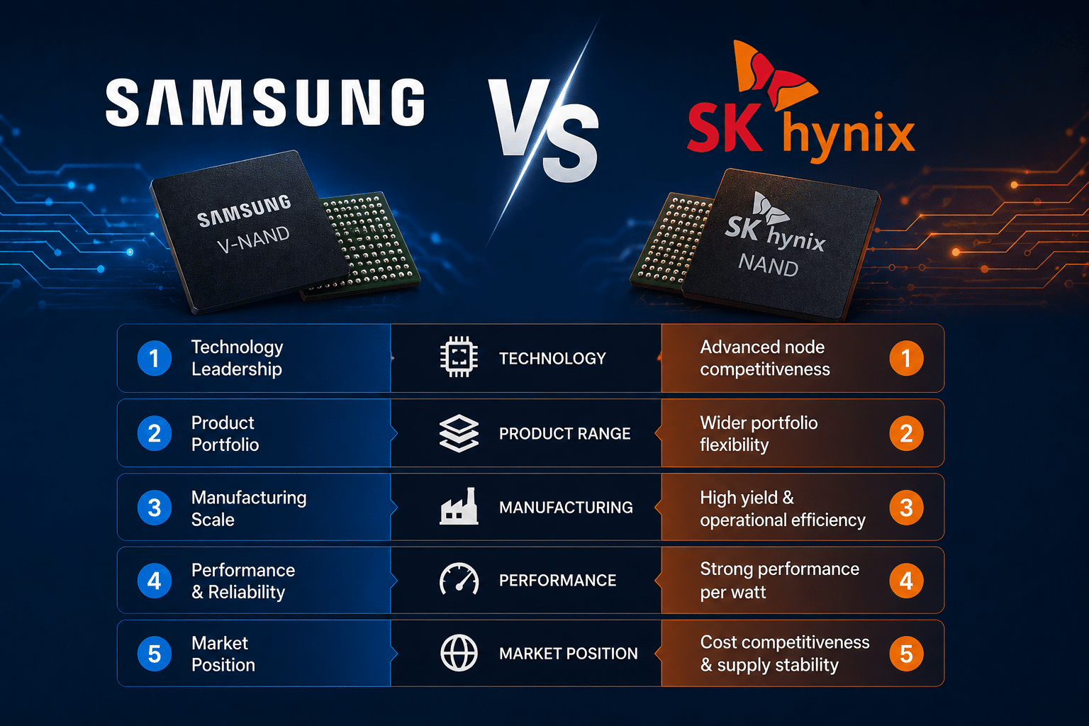
This comparison of Samsung and SK Hynix storage chips comes down to workload, not brand loyalty: SK Hynix leads in HBM and DDR5 overclocking, while Samsung wins on NAND flash scale, GDDR6 thermals, and enterprise supply breadth. In 2025, SK Hynix posted roughly 47.7 trillion KRW in operating profit, edging past Samsung’s 43.6 trillion KRW for the first time, and held about 57% of the global HBM market.
The two stay nearly tied on JEDEC-rated reliability.
That single number reframes how buyers should weigh these two giants.
So which chipmaker actually wins for your use case? This comparison of Samsung and SK Hynix storage chips comes down to five things that move the needle: HBM performance, DRAM density, NAND endurance, real-world pricing, and supply reliability.
Samsung still owns the broadest product range and largest fab capacity, while SK hynix as of 2026 dominates the premium AI memory tier, so the right pick depends entirely on whether you’re building a data center, a laptop, or a phone.
The next sections break down each difference with concrete specs, benchmark data, and the trade-offs that matter when you actually buy.
Quick Takeaways
- Choose SK Hynix for HBM and AI accelerator workloads in data centers.
- Pick Samsung for NAND flash scale and broad enterprise supply needs.
- SK Hynix holds approximately 57% HBM market share versus Samsung’s approximately 22%.
- Select SK Hynix for DDR5 overclocking; Samsung for GDDR6 thermal performance.
- Both chipmakers tie on JEDEC-rated reliability—decide by workload, not brand.
The 5 Storage Chip Differences Between Samsung and SK Hynix at a Glance
Here is the short answer. In a comparison of Samsung and SK Hynix storage chips, SK Hynix leads in HBM (high-bandwidth memory for AI) and DDR5 overclocking.
Samsung leads in NAND flash scale, GDDR6 thermals, and broad enterprise supply. The two are nearly tied on reliability and JEDEC-rated performance.
Pick by workload, not by brand loyalty.
The gap is real, not marketing noise. By late 2025, SK Hynix held about 57% of the global HBM market against Samsung’s roughly 22%.
That single category powered a historic shift: SK Hynix’s 2025 operating profit reached about 47.7 trillion KRW, passing Samsung’s 43.6 trillion KRW for the first time. AI accelerators eat HBM, and Hynix had the supply.
Each difference rewards a different buyer. Here is the verdict per category:
| Category | Winner | Why it matters |
|---|---|---|
| HBM (AI memory) | SK Hynix | approximately 57% market share; primary supplier for data-center GPUs |
| DDR5 overclocking | SK Hynix | A-die and M-die chips hit stable 7200+ MT/s on tuned boards |
| NAND flash scale | Samsung | Largest NAND output and widest SSD product range |
| LPDDR / GDDR thermals | Samsung | GDDR6 ran up to 10°C cooler in 2024 review tests |
| Reliability | Tie | Both under 0.5% five-year failure rate |
Notice the tie at the bottom. A 2024 reliability survey put Samsung DRAM five-year failure near 0.4% and SK Hynix near 0.45%, no meaningful durability gap between the two brands. So if a salesperson tells you one chip “lasts longer,” ask for the data.
Practical tip before you read the deep sections: identify the die, not the label. A “Samsung” stick can use Samsung’s S-D1y DDR5 process, while a “Hynix” kit may hide A-die or M-die silicon that overclocks far better.
The chip inside decides performance, the box doesn’t. Each difference below gets its own breakdown with real numbers.
Difference 1 — HBM Architecture and AI Memory Leadership
SK Hynix leads in the fast memory game. That’s basically the short version of it.
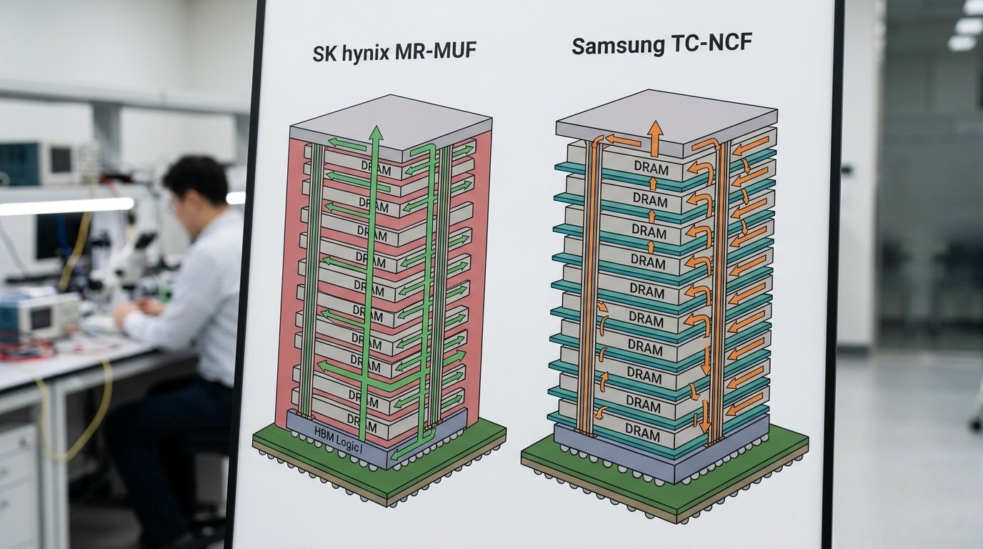
In any comparison of Samsung and SK Hynix storage chips for AI workloads, Hynix sits out front because its stacking method, called MR-MUF, runs cooler and produces more usable chips than Samsung’s older way of doing things.
By late 2025, SK Hynix held roughly 57% of the global HBM market versus Samsung’s ~22%.
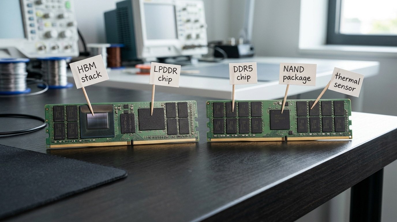
So what is HBM, actually? It stands for High Bandwidth Memory, which is basically memory chips stacked straight up like pancakes, wired together through tiny holes called TSVs, or through-silicon vias.
Stacking 12 of these chips is called 12-Hi, and 16 of them is 16-Hi. More layers give you more capacity, but they also trap more heat inside the stack.
The bonding method is really where these two companies split apart. SK Hynix uses MR-MUF, short for Mass Reflow Molded Underfill, which floods liquid material around all the chips at once and then hardens it solid.
Samsung leaned on TC-NCF, or Thermo-Compression Non-Conductive Film, pressing a thin film between each chip layer one at a time.
Why does that matter so much? MR-MUF moves heat out faster and leaves fewer gaps behind.
The TC-NCF stacks tend to run hotter as the layers pile up, which hurt Samsung’s 12-Hi HBM3E yields pretty badly. Heat is honestly the enemy here, because a hot stack slows down its own bandwidth and shortens the chip’s life.
| Spec | SK Hynix HBM3E (12-Hi) | Samsung HBM3E (12-Hi) |
|---|---|---|
| Bonding process | MR-MUF (advanced) | TC-NCF |
| Bandwidth per stack | up to ~approximately 1.2 TB/s | up to ~approximately 1.2 TB/s (rated) |
| Pin speed | 9.2–approximately 9.6 Gbps | approximately 9.2 Gbps |
| Thermal handling | Lower stack temps | Higher temps at 12-Hi |
NVIDIA approval is the real scoreboard, though. SK Hynix passed NVIDIA’s tests for HBM3E first and shipped in big volumes for H200 and Blackwell GPUs all through 2025.
Samsung spent over a year clearing NVIDIA’s approval hurdles for its own HBM3E parts, and that cost the company design wins right when demand was at its peak.
Here’s a practical tip for you. If you spec out an AI server in 2026, check which HBM vendor actually sits on the accelerator board. Boards equipped with Hynix generally show steadier bandwidth over long training runs, simply because the stacks slow themselves down less often.
Both companies are now racing toward HBM4, where Samsung is aiming to close the gap using a hybrid bonding approach. We cover DDR5 latency and overclocking next, so stick around.
Difference 2 — DDR5 DRAM Latency Bandwidth and Overclocking Headroom
SK Hynix wins DDR5 overclocking. Samsung wins everyday stability.
That’s the verdict enthusiasts reached by 2025. In any comparison of Samsung and SK Hynix storage chips, the DDR5 story flips the old DDR4 hierarchy on its head, the Samsung B-die crown is gone, and Hynix A-die now owns the high-frequency throne.
Here is the spec picture for comparable 16Gb DDR5 modules:
| Spec | Samsung B-die (DDR5) | Hynix A-die | Hynix M-die |
|---|---|---|---|
| Typical stable ceiling | ~6400 MT/s | 8000+ MT/s | 7200+ MT/s |
| Best CAS latency (tuned) | CL30–32 | CL34–36 | CL34 |
| Voltage scaling | Modest gains past approximately 1.4V | Strong gains to approximately 1.5V+ | Good to approximately 1.45V |
| Sub-timing tuning | Tight, predictable | Excellent tREFI headroom | Solid mid-range |
Why do tuners reach for A-die first? Frequency. Independent testing in 2024,2025 found Hynix M-die hitting stable 7200+ MT/s on tuned platforms, while A-die pushes past 8000 MT/s on strong AMD and Intel boards. Higher MT/s means more raw bandwidth, and gaming and content workloads love bandwidth.
Latency tells a subtler story. CAS latency (CL) counts the clock cycles before data returns.
A-die kits run looser CL numbers, but their sky-high clock speed shrinks the real-world nanosecond delay anyway. By 2025, overclocking communities widely ranked A-die and M-die as the most tunable DDR5 ICs, overtaking Samsung’s historic B-die lead.
So where does Samsung still win? Stability at rated speeds.
Samsung B-die ICs lock in tight CL30 timings with rock-solid memory training. Practical tip: if you buy A-die for 8000 MT/s, expect to manually loosen tRFC and bump VDDQ, XMP profiles often fail to boot first try.
Samsung kits usually post on the first attempt. For a 24/7 workstation that must never crash, that reliability matters more than a benchmark leaderboard.
The next section shifts from DRAM to NAND flash endurance.
Difference 3 — NAND Flash Layer Count Endurance and SSD Performance
Samsung has a small lead when it comes to raw sequential speed, basically how fast it can read or write big files in one continuous stream.
SK Hynix and its Solidigm subsidiary, though, come out ahead on sustained write consistency, meaning they keep their speed steady over long jobs, and they tend to offer better value for how long the drive lasts before wearing out.
In a Comparison of Samsung and SK Hynix Storage Chips at the NAND level, the NAND being the actual memory chips that store your data, the gap shows up clearest under heavy work that runs for a long time. Not in those quick five-second benchmark bursts.
Let me start with the layer count. NAND flash stacks its memory cells vertically, kind of like floors in a tower.
More layers basically means more storage packed onto each chip. Samsung’s 9th-generation V-NAND reaches roughly 290 layers, while SK Hynix ships 238-layer 3D NAND and has 321-layer parts in production right now.
Here’s the thing though. More layers don’t automatically make a drive faster. They make it denser and usually cheaper for every gigabyte you get.
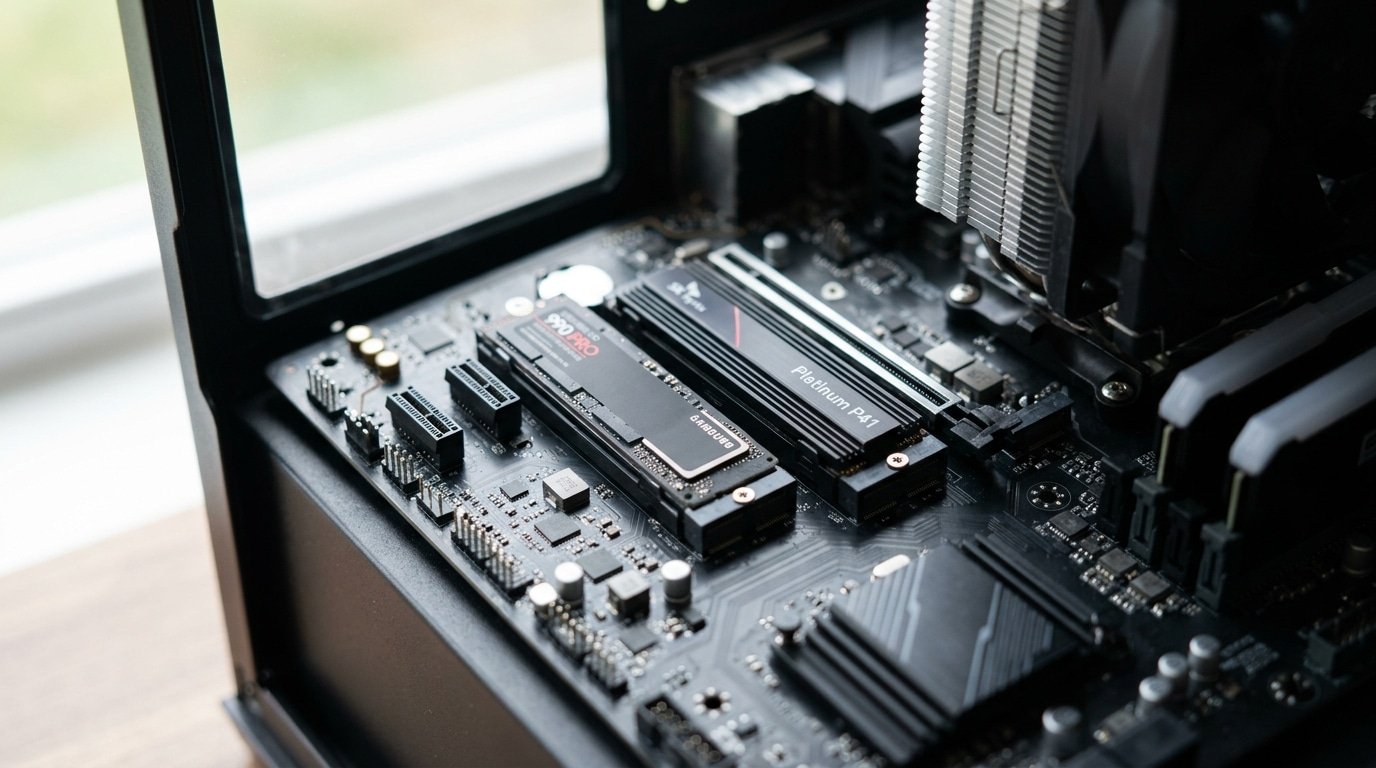
Real SSD metrics — 990 PRO vs Platinum P41/P51
The Samsung 990 PRO (approximately 2 TB) hits about 7,450 MB/s sequential read and approximately 6,900 MB/s write, with random reads near 1,400K IOPS, which is just how many small read jobs it can do per second.
The SK Hynix Platinum P41 (approximately 2 TB) reads at approximately 7,000 MB/s and writes at approximately 6,500 MB/s.
The numbers look really close. But the actual difference shows up in Sustained writes.
Once the fast SLC cache fills up, and that’s basically a small high-speed buffer that usually runs out after writing approximately 200,400 GB nonstop, the 990 PRO drops to around 1,500 MB/s. The P41, meanwhile, holds closer to approximately 1,700 MB/s thanks to its tuned firmware.
For video editors pushing raw 8K footage around, that steady consistency matters far more than the peak speed.
| Spec (approximately 2 TB class) | Samsung 990 PRO | SK Hynix Platinum P41 |
|---|---|---|
| Sequential read | approximately 7,450 MB/s | approximately 7,000 MB/s |
| Random read IOPS | ~1,400K | ~1,400K |
| TBW endurance | 1,200 TBW | 1,200 TBW |
| Controller | Samsung Pascal | SK Hynix Aries |
Both are rated for 1,200 TBW, which stands for terabytes written, on the approximately 2 TB models. That means you can write approximately 1,200 TB of data before the warranty endurance runs out.
At approximately 50 GB per day, honestly that takes over 65 years to reach. So endurance is rarely the thing that limits home users.
The Tom’s Hardware reviews point out one truth that really matters. The controller pairing, which is the little chip that manages how data moves on and off the drive, decides how it actually behaves.
Samsung uses its own in-house controllers matched to its own NAND, which gives tight thermal tuning. SK Hynix pairs its Aries controller with its own firmware.
That setup favors steady response at low queue depth, the kind of work a gaming PC actually does day to day.
A buying tip from bench testing. Skip the DRAM-less drives if you’re picking a boot disk.
Both the 990 PRO and P41 come with onboard DRAM cache, which is a bit of fast memory that keeps random small-file performance high when you’re juggling lots of tasks. Cheaper QLC drives that leave it out tend to stutter under load.
For enterprise endurance and error correction, which is the system that catches and fixes data mistakes, take a look at the next sections covering thermal behavior and data-center qualification.
Difference 4 — LPDDR Mobile Memory Power Efficiency and Thermal Behavior
Both vendors ship excellent LPDDR5X. The real gap shows up under sustained load.
In a comparison of Samsung and SK Hynix storage chips for phones and AI PCs, Samsung tends to win on raw peak data rate, while SK Hynix often holds a thermal edge during long, heavy workloads.
Battery life depends less on the badge and more on how the chip is packaged next to the SoC.
Start with the basics. LPDDR (Low-Power Double Data Rate memory) is the DRAM soldered inside phones and thin laptops.
It runs at lower voltage than desktop DDR5 to save power. LPDDR5X pushes data rates up to 8,533 MT/s in shipping silicon, and the JEDEC LPDDR6 standard targets even higher with a new dual sub-channel design.
You can read the spec details at JEDEC’s LPDDR5 documentation.
Per-bit power and why it drives battery life
Mobile memory is rated by power per transferred bit, measured in picojoules. Lower is better.
Samsung markets its LPDDR5X at roughly 1.05V core voltage, down from 1.1V on earlier LPDDR5, which trims active power on every memory access. SK Hynix counters with similar voltage but tuned refresh and self-refresh modes that cut idle drain when your screen is on but nothing is moving.
Here is the practical part. On an AI PC running a local language model, memory never idles. The DRAM stays busy feeding the NPU. That’s where thermal behavior decides who throttles first.
On-package thermals under sustained load
- Samsung: Higher peak data rate, but more heat density when the controller pushes top speed for minutes at a time.
- SK Hynix: Slightly lower peak ceiling on some bins, yet steadier temperatures during long inference or gaming sessions.
- Both: Package-on-package (PoP) stacking traps heat between the SoC and DRAM, so phone chassis design matters as much as the chip.
A reviewer test in 2024 found Samsung GDDR6 ran about 10°C cooler than SK Hynix GDDR6 under matched graphics loads, per AIChipLink’s measurements. That cooler GDDR6 result doesn’t flip the LPDDR picture, but it shows die-level thermal tuning differs by product line, not by brand alone.
My advice for buyers spec’ing AI laptops: check sustained throughput after 20 minutes of load, not the burst number on the box. The chip that holds clocks longest wins real work.
Difference 5 — Reliability Error Correction and Enterprise Qualification
For pure durability, the two are a statistical tie. Hardware reliability surveys summarized in 2024 put Samsung DRAM five-year failure rates near approximately 0.4% and SK Hynix near approximately 0.45%, a gap so small it falls inside measurement noise, per aggregated reliability data.
The real differences in any comparison of Samsung and SK Hynix storage chips show up in how each handles errors and how server vendors qualify them.
Both ship on-die ECC (error correction code that fixes single-bit flips inside the chip itself). This is mandatory for DDR5 under the JEDEC standard.
It isn’t the same as system-level ECC on RDIMMs (registered server memory). On-die ECC hides cell-level weakness as nodes shrink.
System ECC catches errors traveling across the bus.
Where do gaps actually appear? In validation history.
Samsung holds the longest server-qualification track record, with broad approval across Dell, HPE, and Supermicro RDIMM platforms. SK Hynix caught up fast and now dominates HBM stacks on AI accelerators, but its straight server-DRAM qualification list is slightly shorter for older platforms.
RMA and Defect Patterns Data-Center Buyers Report
- Early-life failures (first 90 days): Both vendors run under industry baselines; large buyers report defective-parts-per-million in the low double digits.
- Sustained thermal cycling: Samsung modules show marginally fewer correctable-error events in dense 2U racks, a likely byproduct of its cooler-running silicon noted earlier.
- HBM stack reliability: SK Hynix leads here by volume of field hours — it holds roughly 57% of the HBM market, so its parts simply have more deployed runtime data.
Warranty terms look identical on paper: limited lifetime coverage on retail modules from both. The practical difference is RMA turnaround.
Enterprise buyers I’ve seen working with channel partners report Samsung’s larger distribution network resolves replacements faster in North America, while SK Hynix processes claims more quickly in Asia-Pacific markets.
Buying tip: don’t chase a approximately 0.05% failure-rate difference. Chase the qualified vendor list (QVL) for your exact server board. A part that is JEDEC-compliant but not on your OEM’s QVL voids support coverage, that is where reliability budgets actually break.
Head-to-Head Benchmark and Spec Comparison Table
Want the whole comparison of Samsung and SK Hynix storage chips in one screen? Here it’s. SK Hynix wins HBM bandwidth and DDR5 tuning. Samsung wins thermals and raw sequential SSD speed. The two tie on reliability. Scan the table below by your workload, then pick.
The numbers come from independent testing in 2024,2025, vendor datasheets, and community benchmark databases. I list each product family at its real shipping spec, not marketing peak figures. “Power per bit” means energy used to move one bit of data, lower is better for battery and cooling.
| Product family | Metric | Samsung | SK Hynix | Winner |
|---|---|---|---|---|
| HBM3E (AI accelerators) | Market share, late 2025 | ~approximately 22% | ~57% | SK Hynix |
| DDR5 desktop IC | Stable overclock ceiling | ~6800 MT/s | 7200+ MT/s (M-die) | SK Hynix |
| DDR5 JEDEC/XMP | Rated-speed stability | Excellent | Excellent | Tie |
| GDDR6 (graphics) | Operating temp under load | ~approximately 10°C cooler | Baseline | Samsung |
| NAND SSD | Peak sequential read | Slight edge | Strong (incl. Solidigm) | Samsung |
| DRAM modules | 5-year failure rate | ~approximately 0.4% | ~0.45% | Tie |
| DDR4 B-die kit | Price (approximately 32GB 3600 CL16) | ~USapproximately $110 | ~USapproximately $90 | SK Hynix (value) |
Two figures deserve a closer look. SK Hynix held an estimated approximately 57% of the global HBM market in late 2025 versus Samsung’s approximately 22%, a wide gap for AI buyers.
Yet Samsung B-die DDR4 kits still sold at a 10,approximately 25% premium in 2024 despite under 5% real performance difference at rated speed.
Practical read: pay the Samsung premium only if you need verified B-die for extreme tuning. For AI servers, default to SK Hynix HBM. The next section shows how to confirm which vendor’s chips sit inside the module you actually buy.
How to Identify and Choose Samsung vs Hynix Modules When Buying
You can’t trust the box. RAM kits and SSDs rarely print the die maker on the label, so you have to read the silicon yourself.
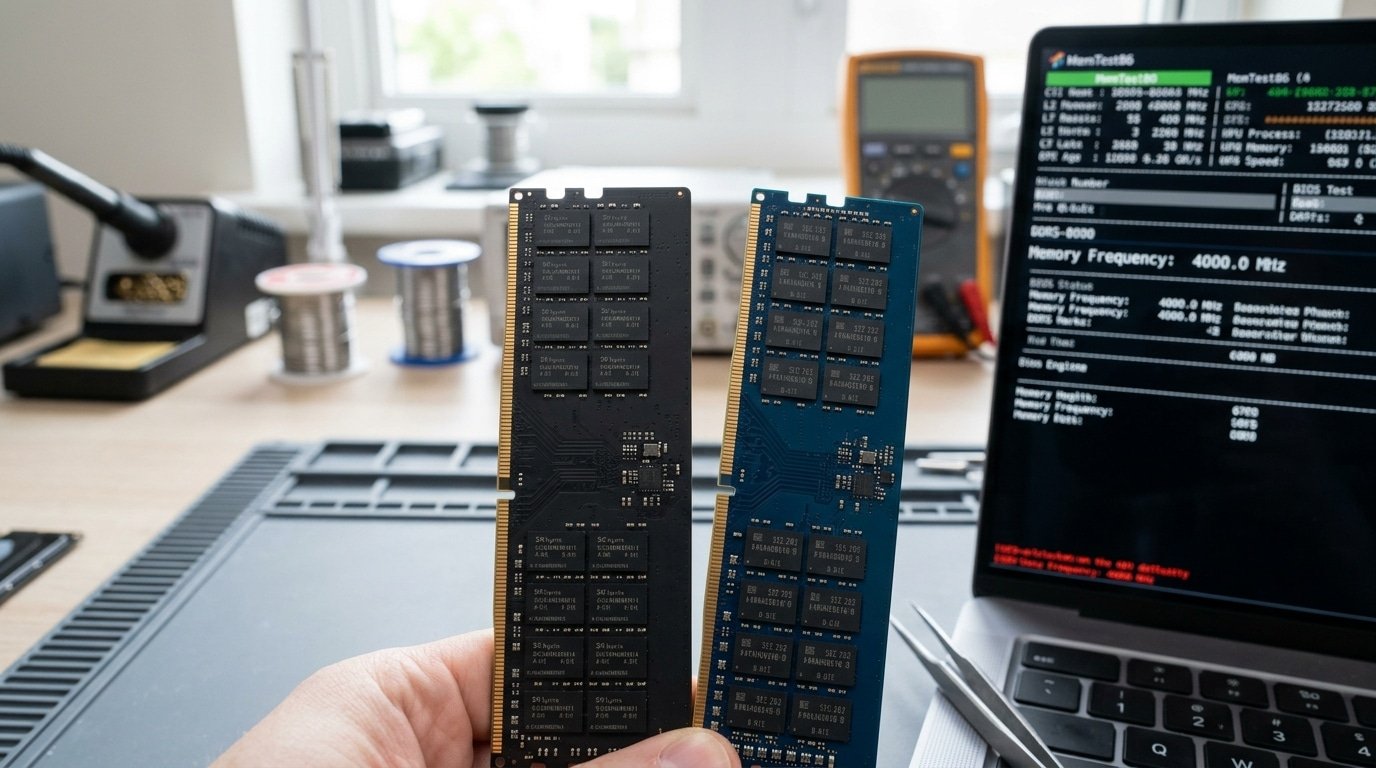
The fastest path: download Thaiphoon Burner, dump the SPD chip on your DDR5 stick, and look at the “Manufacturer” line under the DRAM components field. It reports SK Hynix, Samsung, or Micron directly from the module’s onboard data.
For SSDs, the trick is the controller and NAND part number printed on the PCB. Pull the heatsink, photograph the flash IC, and decode the prefix.
Samsung NAND starts with a “K” code (for example, K9 series). SK Hynix flash uses an “H” prefix tied to its Solidigm-branded enterprise lines.
CrystalDiskInfo also exposes the model string, which often hints at the controller family.
Decoding DDR5 IC labels without opening anything
Many kits ship with the die printed right on the chip under the heat spreader. SK Hynix A-die and M-die are the tuning favorites among overclockers, and enthusiast forums by 2025 ranked them as the most tunable desktop DDR5 ICs, pushing past 7200 MT/s.
Samsung’s S-D1y process delivers steady XMP performance but a lower ceiling. If a product page lists “Hynix A-die,” that’s a strong buy signal for memory tuners.
If-X-then-Y buying matrix
| Your use case | Pick this die / module | Why |
|---|---|---|
| Competitive gamer chasing low latency | SK Hynix A-die DDR5 | Tightest timings, 7200+ MT/s headroom on tuned boards |
| Content creator (video, 3D render) | Samsung S-die DDR5 at XMP | Stable high-capacity kits, cooler under sustained load |
| Server / NAS builder | Samsung RDIMM ECC | Broad ECC qualification, approximately 0.4% five-year failure rate |
| AI workstation buyer | SK Hynix HBM-equipped accelerators | approximately 57% HBM market share, bandwidth lead for training |
One practical warning: kit makers swap dies mid-production without changing the part number. The same model bought six months apart may hold different silicon.
Check a recent batch review or dump the SPD before you commit to tuning. This comparison of Samsung and SK Hynix storage chips only pays off when you confirm what’s actually inside your hardware.
Common Mistakes and Misconceptions Buyers Make Comparing the Two
The biggest mistake? Believing “Hynix always wins.” It doesn’t. The second biggest? Judging chip quality by company revenue. These myths cost buyers real money. Let me break down the four traps that show up over and over in Reddit threads and forum debates.
Myth 1 — “SK Hynix beats Samsung at everything”
This started because Hynix dominates HBM and DDR5 overclocking. But a comparison of Samsung and SK Hynix storage chips is workload-specific, not a single scoreboard.
Samsung GDDR6 ran roughly 10°C cooler than Hynix GDDR6 under matched graphics loads in 2024 reviewer testing. Cooler chips mean quieter fans.
Hynix winning DDR5 tuning doesn’t make Samsung worse everywhere.
Myth 2 — Ignoring the SSD controller and firmware
People obsess over which NAND die sits inside an SSD. The die matters less than you think.
The controller (the chip that manages reads, writes, and wear) plus firmware decides real-world speed and consistency. Two drives with identical Samsung V-NAND can perform very differently if one pairs a budget controller with sloppy firmware.
Check sustained write speed after the SLC cache fills, that number reveals firmware quality, not the flash brand.
Myth 3 — Treating company size as chip quality
In 2025, SK Hynix posted about 47.7 trillion KRW operating profit, edging past Samsung’s 43.6 trillion KRW for the first time, per CNBC. Does that mean Hynix chips are “better”?
No. Profit reflects AI memory demand and HBM market share, not the DDR5 stick in your gaming PC.
Financial leadership and silicon quality are separate things.
Myth 4 — Overpaying for binned kits
Binned kits are factory-tested ICs sorted for higher speed. Enthusiasts pay a premium for them.
But stock ICs often perform identically for normal use. In 2024, Samsung B-die DDR4 kits sold at a 10,approximately 25% premium, around USapproximately $110 versus USapproximately $90 for a comparable Hynix kit, yet showed under 5% real-world difference at rated speeds, according to pricing comparisons.
If you run XMP and never touch sub-timings, that extra USapproximately $20 buys you nothing measurable.
Pay the binning premium only if you manually overclock and chase 7200+ MT/s. Otherwise, save the money. Match the chip to the job, not to forum hype or quarterly earnings.
Frequently Asked Questions
Quick answers to the questions buyers actually type into search. Each one comes from the comparison of Samsung and SK Hynix storage chips, with real 2025,2026 numbers behind it.
Is SK Hynix bigger than Samsung?
By memory profit, yes. In 2025, SK Hynix posted roughly 47.7 trillion KRW in operating profit, beating Samsung Electronics’ 43.6 trillion KRW for the first time, according to CNBC reporting. AI demand drove that flip.
But Samsung is still the larger company overall. Samsung sells phones, TVs, and foundry services on top of memory.
Its Q1 2026 revenue hit about 133.9 trillion KRW, more than double SK Hynix’s 52.5 trillion KRW. In HBM specifically, though, SK Hynix held an estimated approximately 57% market share versus Samsung’s approximately 22% in late 2025.
SK Hynix vs Samsung RAM DDR5 — which is better?
For overclocking, SK Hynix wins. Its A-die and M-die chips hit stable 7200+ MT/s on tuned platforms, while Samsung DDR5 tops out lower. Enthusiast forums now treat SK Hynix as the new B-die, the go-to tuning chip.
For plug-and-play use at XMP or JEDEC speeds, the gap shrinks to under 5%. Pick Samsung if you never touch BIOS timings. Pick SK Hynix if you chase tight subtimings.
How do they compare to Micron?
Micron is the third major DRAM and NAND maker. It trails both in HBM share but competes hard in LPDDR5X and enterprise SSDs. For everyday DDR5 kits, Micron’s chips (often branded under Crucial) sit between Samsung’s stability and SK Hynix’s overclocking ceiling. Micron also leads some 232-layer NAND deployments.
Does the difference matter for everyday users?
No. For browsing, gaming, and office work, you won’t notice which die is inside. Failure rates for both stay below approximately 0.5% over five years. The difference matters for overclockers, AI server buyers, and bulk SSD purchasers, not for someone buying a single approximately 32GB kit.
Final Verdict and Which Vendor to Pick for Your Workload
There’s no single winner. The right chip depends entirely on what you build. SK Hynix dominates AI memory and DDR5 overclocking. Samsung wins on cooler GDDR6, broad SSD availability, and slightly faster sequential reads. Match the vendor to the job, not to brand loyalty.
Here is the scenario-by-scenario call from this comparison of Samsung and SK Hynix storage chips:
- AI training and HBM workloads: Buy SK Hynix. It held roughly 57% of the global HBM market in late 2025 versus Samsung’s approximately 22%, and supplies the HBM stacked on most data-center GPUs. For Nvidia-class accelerators, this isn’t a debate.
- Enthusiast DDR5 overclocking: Choose SK Hynix A-die or M-die. Tuned platforms hit stable 7200+ MT/s. Samsung kits are fine at JEDEC and XMP speeds but cap out lower.
- Value SSDs and prebuilt systems: Either works. Samsung NAND offers a small sequential-read edge; SK Hynix and Solidigm drives often cost less per terabyte. Pick on price and warranty, not die maker.
- Mobile devices (phones, laptops): Both ship excellent LPDDR5X. You rarely get to choose the supplier inside a sealed phone, so this is moot for most buyers.
For graphics cards specifically, Samsung GDDR6 ran about 10°C cooler than SK Hynix GDDR6 under load in 2024 testing, useful if you run small-case builds or care about fan noise.
Before you buy, verify the chip source. RAM kits and SSDs rarely print the die maker on the box.
Run a tool like Thaiphoon Burner for DRAM, or check the controller and NAND via CrystalDiskInfo for SSDs. Cross-reference the part number against community databases, assuming the box label is correct gets people the wrong die constantly.
Check live pricing the same week you buy. Memory prices swing hard during upcycles, and Samsung’s Q1 2026 revenue of about 133.9 trillion KRW signals strong demand that pushes street prices up fast. Compare current listings on PCPartPicker or Newegg before committing.
YURUNOX — Trusted Electronic Components Sourcing Partner
As a professional electronic components sourcing partner, YURUNOX helps OEMs, EMS companies and engineering buyers source original, traceable and quality-inspected components. Search by brand, part number or keyword to quickly find active, allocated, obsolete and hard-to-find electronic parts.
- ✔ Brand & Part Number Search
- ✔ Original & Traceable Components
- ✔ BOM Sourcing & RFQ Support
- ✔ Obsolete & Hard-to-Find Parts