

How to Choose an ADC: Resolution, Speed, Accuracy
Start with the measurement you need, not the number of bits on the box. Match input range, noise, usable sample rate and total error before choosing an analog-to-digital converter.

How to choose an ADC: define the signal, error and timing first
Choose an ADC by specifying input range, smallest useful change, allowable measurement error and valid samples per second per channel. Then check noise, linearity, settling, latency and the supporting circuit at the intended operating conditions. Resolution, speed and accuracy answer different questions; none replaces the others.
Resolution: how finely the input is divided into nominal digital steps.
Noise: how much readings fluctuate and which small changes remain usable.
Speed: when valid information becomes available, not just the clock rate.
Accuracy: how far the complete measurement can be from the true value.
Replace a component wish list with a measurement requirement
“We need a 16-bit ADC” is not enough to select a part. An illustrative requirement is: “Measure a 0–4 V sensor output within ±2 mV, deliver 100 valid readings per second, and maintain that performance across the specified operating temperatures.”
State whether the error limit covers the converter alone, the electronics, or the instrument including its sensor. Also define the smallest change separately from absolute error. A repeatable 0.1 mV change can be useful even in an instrument with a larger calibrated uncertainty.
Swipe horizontally to compare the details.
| Requirement | Record it in useful units | What it changes |
|---|---|---|
| Signal and overload | Minimum, maximum, polarity and abnormal levels | Input range, gain, protection and pin limits |
| Smallest useful change | Volts or sensor units at a defined bandwidth | Code spacing and noise target |
| Allowed error | Limit, temperature range and calibration state | Reference, linearity and system error budget |
| Bandwidth and response | Wanted frequencies and maximum acceptable delay | Sampling, filtering and latency |
| Channels and timing | Valid rate per channel; scan or simultaneous capture | Converter count, settling and synchronization |
| Integration constraints | Supply rails, host interface, power and footprint | Complete implementation and sourcing options |
Missing requirements are questions to resolve. More bits cannot fix an undefined error target, and a smoother display is not necessarily a faster measurement.
Resolution is a starting point, not an accuracy guarantee
An ideal N-bit ADC has 2N code bins across its input span. One least significant bit (LSB) represents the nominal code width:
Use the span, not automatically the reference voltage. A range from −2.048 V to +2.048 V spans 4.096 V. Gain, coding and the actual transfer function determine how the input maps into codes.
Swipe horizontally to compare the details.
| Nominal bits | Code bins | Ideal LSB |
|---|---|---|
| 12 | 4,096 | 1 mV |
| 16 | 65,536 | 62.5 µV |
| 24 | 16,777,216 | About 0.244 µV |
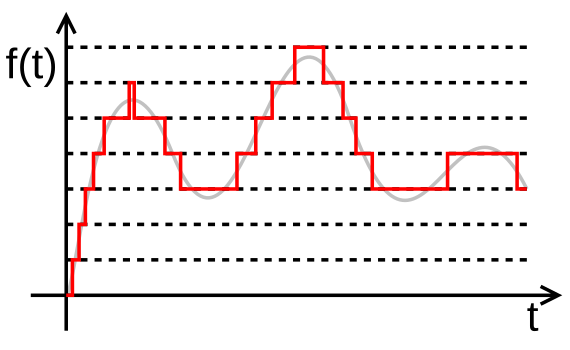
One step per change is a thin starting margin
A 1 mV change spans only one ideal step in the 12-bit example. That is a screening result, not proof the change can be detected reliably in noise.
The familiar ideal in-range quantization model uses a half-LSB error bound. Actual converters add noise and transfer errors. See Analog Devices MT-001 for the assumptions behind the ideal model.
Use the input range before paying for more bits
Illustrative small-signal example: a 20 mV signal span uses only about 320 nominal code widths on the 16-bit, 4.096 V converter. A gain of 32 expands that to about 10,240 code widths. The input-referred step falls from 62.5 µV to about 1.953 µV.
A programmable gain amplifier (PGA) or external amplifier may therefore be useful. Its noise, offset, drift and headroom still matter. Check both input endpoints and common-mode voltage: a span that fits mathematically can still sit outside the permitted input window.
ADC resolution and gain calculator
An ideal code-width screening tool
Compare nominal bits and ideal gain against your signal. The result does not model noise, accuracy, settling, pin limits or real amplifier performance.
- Ideal input-referred LSB
- 62.5 µV
- Nominal code widths across the signal
- 320
- Code steps per required change
- 16
- Minimum bits for one step per change
- 12 bits
The amplified signal spans 0.488% of the ADC range.
The ideal code width is smaller than the requested change. Check noise and the accuracy budget before selecting the part.
Calculation basis: input-referred LSB = span ÷ (2N × gain). Code widths used = signal span × gain ÷ LSB at unity gain. Minimum bits are rounded up for an LSB no larger than the requested change, with a minimum of one bit. This is not a noise-free-bit or ENOB calculation.
Noise, DC effective resolution and ENOB are different measures
A steady analog input can produce changing output codes. For a slow sensor, input-referred noise in microvolts at the intended gain and bandwidth is often more useful than the output word length.
Use the same input reference point for span and noise. Peak-to-peak noise depends on observation time and filtering; there is no universal RMS-to-peak-to-peak factor. “Noise-free” does not mean a code can never change. Analog Devices explains these DC noise metrics.
For waveforms, compare ENOB under matching conditions
This conventional relationship uses a full-scale sine-wave basis. Account for amplitude normalization when the test signal is below full scale. An illustrative SINAD of 78 dB gives about 12.66 bits, even if the converter outputs a 16-bit word.
Compare input frequency, amplitude, sample rate and measurement bandwidth. SNR normally excludes harmonic distortion; SINAD includes it. Dynamic ENOB does not establish DC offset, gain accuracy or drift. See Analog Devices on AC behavior and ENOB.
Read the noise row for the mode you will actually use
Record the rate, gain, filter, supply, input connection and whether the value is typical or a guaranteed limit. A shorted-input typical result helps compare converters, but it does not include sensor noise, wiring pickup or the complete board. The ADS1220 example below shows how much one setting can change the comparison.
A small LSB can hide a large measurement error
Accuracy is not simply 1 ÷ 2N. Offset shifts the transfer curve; gain error changes its slope; integral nonlinearity (INL) describes deviation from a specified straight line. Differential nonlinearity (DNL) describes variation in individual code widths. Check the manufacturer's line-fitting and endpoint definitions.
Temperature adds another dimension. A no-missing-codes specification or a good room-temperature noise result does not establish the complete error limit over temperature. Analog Devices MT-010 distinguishes the static transfer specifications.
The 16-bit reading that still misses a ±1 mV requirement
A 16-bit, 4.096 V span has a 62.5 µV LSB. In an uncalibrated, nonratiometric system, a 0.1% reference-scale error contributes approximately 4 mV at a 4 V input. That term alone is larger than an assumed ±1 mV total-error limit.
The useful next question is whether reference selection or calibration can reduce the residual scale error. Changing to a 24-bit converter without addressing it only gives a more finely divided wrong result.
Put every error at the same point and in the same units
- Choose a common unit: input-referred volts, sensor units, or a defined fraction of full scale.
- Separate percent of reading from percent of full scale. Their contribution differs, particularly near zero input.
- Keep deterministic limits separate from random noise. Sum applicable worst-case magnitudes conservatively; combine independent, compatible RMS noise terms by root-sum-square.
- Avoid double counting. A total-error specification may already contain offset, gain and linearity contributions.
Define the acceptance rule for noise and uncertainty. A typical RMS value cannot be inserted into a guaranteed worst-case sum without a statistical interpretation.
Calibrate the errors you can actually reach
Internal calibration addresses supported converter errors. System calibration can include some external errors when the specified known inputs are applied at the correct point. Analog Devices AN-1464 shows why these procedures are not interchangeable.
Record the calibration source's uncertainty, temperature, production time, coefficient storage and recalibration interval. Calibration does not automatically remove random noise, all nonlinearity or subsequent drift. If production cannot perform the proposed calibration, select against the achievable uncalibrated budget.
Choose sampling rate with the filter and channel schedule
For conventional baseband sampling, the ideal Nyquist condition requires a sample rate above twice the highest retained frequency. Real anti-alias filters need a transition band, so choosing exactly 2× the wanted bandwidth is not a complete design.

Illustrative vibration requirement: for a 2 kHz wanted bandwidth, the ideal threshold is above 4 kSPS. A candidate rate of 10 or 20 kSPS gives more room for a practical filter, but neither is approved until the filter response and out-of-band interference are evaluated. Analog Devices MT-002 covers the sampling and filtering relationship.
Separate sampling, output rate and latency
- Sampling: when the analog signal is captured.
- Output data rate: how often a new result is delivered.
- Latency: how old that information is when the system can act on it.
A delta-sigma converter's modulator runs faster than its delivered output rate. Digital filtering and decimation affect noise, bandwidth and response. Review first-conversion behavior, group delay, settling after a channel or gain change, readout time and host scheduling. A smooth but stale measurement can fail a control-loop requirement.
Four channels at 20 kSPS are not a 20 kSPS job
An illustrative four-channel system requiring 20,000 valid samples per second per channel needs at least 80,000 valid results per second in aggregate. A nominal 100 kSPS converter offers 25 kSPS per channel only in an ideal equal scan without additional overhead or discarded data.
- 01 / SELECTSwitch the channelAllow the input path to respond to the new voltage.
- 02 / SETTLE AND CONVERTReach the error targetCheck acquisition and filter behavior at the largest channel step.
- 03 / ACCEPTRead a valid resultAccount for discarded conversions, transfer and scheduling.
Some operations can overlap; others cannot. Build the schedule from the device's timing diagram, not by adding every datasheet interval blindly. If channels must represent the same instant, compare simultaneous sampling and channel skew. A fast sequential scan is not automatically equivalent.
A real trade-off: better noise, slower settling
Changing the driver network changed two selection criteria
TI's 16-bit, 1-MSPS multiplexed reference design includes the input filter, multiplexer, SAR driver, ADC and reference drive. Its report compares the original 5 kΩ driver gain resistors with a 3.48 kΩ modification.
Swipe horizontally to compare the details.
| System result | Original network | Modified network |
|---|---|---|
| Settling time | 390 ns | 1,330 ns |
| DC effective resolution | 15.72 bits | 16 bits |
| Dynamic ENOB | 13.57 bits | 14.33 bits |
The report attributes the improvement to lower driver-network noise, while increased clamp-diode current produces more voltage droop and slower settling. The original AC test uses a full-scale 10 kHz sine wave; DC resolution comes from a separate midscale measurement.
Selection lesson: a lower-noise input circuit can make a fast scan harder to settle. Recheck both requirements after changing the surrounding components.
These are TI's measurements for its documented setup, not YURUNOX tests or guarantees for another board. Read the design report, sections 6 and 7.
SAR, delta-sigma or pipeline: start with the job
Swipe horizontally to compare the details.
| Architecture | Useful starting point | Trade-off to verify |
|---|---|---|
| SAR | Triggered capture, control and multiplexed acquisition | Input acquisition, source drive and conversion timing |
| Delta-sigma | Precision sensing and low-noise filtered measurements | Usable bandwidth, digital filter response and latency |
| Pipeline or pipeline-based | High-rate waveform capture and communications | Pipeline delay, data interface and system power |
A successive-approximation register (SAR) converter determines its code through successive comparisons. Delta-sigma conversion uses oversampling and noise shaping, usually followed by digital filtering. Pipeline conversion distributes work across stages to sustain throughput.
Products overlap in capability. Avoid rules such as “all delta-sigma ADCs are slow” or “SAR always means low power.” Analog Devices compares the architecture mechanisms; use current device specifications for the actual operating envelope.
Do you need an external ADC at all?
Evaluate the microcontroller's integrated ADC against the same requirement sheet. It may reduce part count, but integration does not define measurement quality. Check noise, reference behavior, acquisition time, pin loading, supply coupling and temperature limits before deciding that an external converter is necessary.
Check input headroom, reference drive, clock and data transfer
Check both input pins, not only their difference
A small differential voltage does not prove valid input conditions. Write down each pin's absolute voltage and the common-mode level. Check PGA headroom, source impedance, bias-current paths, protection leakage, startup and what happens when the sensor or ADC is unpowered.
A SAR input sampling network must charge accurately within its acquisition window. A high-value divider, slow amplifier or poorly chosen input filter can make the first reading after a channel change wrong even when the DC transfer looks acceptable. Follow the selected device's input-drive guidance.
A reference must remain accurate while driving the ADC
The reference establishes the voltage scale. Initial error, drift and noise matter, but so do transient load and decoupling. Some SAR reference inputs draw charge during conversion; a reference that looks correct on a multimeter may still move during a conversion burst.
Analog Devices on precision SAR reference design explains the drive problem. Internal and external references both need evaluation against the system budget. For a suitable resistive sensor, a ratiometric excitation/reference arrangement can cancel common variation, but only within the circuit's actual matching and noise assumptions.
Clock jitter becomes important as the signal gets faster
Here fin is sine-wave input frequency in hertz and tj is total RMS sampling-time jitter in seconds. An illustrative 10 MHz input with 1 ps jitter gives about 84 dB. This is a jitter-only limit, not the complete converter SNR. Analog Devices MT-007 explains the model and sampling-time terms.
Budget the link and the energy per valid reading
Four channels at 20 kSPS and 16 useful bits per sample produce 1.28 Mbit/s of payload before commands, status, padding or idle time. Do not equate payload bit rate with the required serial clock. Check the protocol, readout window and the host's ability to keep up.
Add ADC, driver, reference, clock and interface power. For duty-cycled measurements, include wake-up and settling energy as well as the active current. Saving standby power is not useful if every wake-up makes the first required result invalid.
Two ADC datasheets show what headline specifications omit
ADS8866: a 16-bit SAR still needs a timing and drive review
TI's ADS8866 specifies 16-bit conversion at 100 kSPS, a nominal 0-to-VREF input range and an external reference range of 2.5–5 V. Its “no latency output” feature means no extra pipeline conversion delay; acquisition, conversion and readout still take time.
Use those facts to screen a candidate, then verify the input circuit, reference, guaranteed error limits and scan schedule. They do not establish that four multiplexed channels will meet a specified valid rate. Source: ADS8866 datasheet, Rev. C.
ADS1220: 24 bits, but different noise at different rates
The ADS1220 is a 24-bit delta-sigma ADC with a PGA. Its May 2026 datasheet gives these typical input-referred noise values at gain 128:
Swipe horizontally to compare the details.
| Output rate | RMS noise | Peak-to-peak noise |
|---|---|---|
| 20 SPS | 0.09 µV | 0.41 µV |
| 1,000 SPS | 0.70 µV | 4.01 µV |
Conditions: AVDD = 3.3 V, AVSS = 0 V, internal 2.048 V reference, 25 °C, internally shorted inputs and approximately 0.75 seconds of observation on one device. The converter also provides simultaneous 50/60 Hz rejection at 20 SPS.
Buying implication: the lowest-noise row does not describe every speed. A slow precision channel and a fast scan can need different settings, even on the same ADC. These typical figures do not include the sensor or board. Source: ADS1220 datasheet, Rev. D.
Validate the complete signal chain before purchasing
Compare two or three candidates against one requirement sheet. Record exact ordering code, datasheet revision, supply, range, gain, rate, filter, temperature, calibration state and typical versus guaranteed limits. Preserve failed requirements as explicit gaps rather than hiding them behind a higher bit count.
- Check static error across the range.Use known input levels and a reference method with suitable uncertainty. Evaluate residual error under the planned calibration state.
- Measure noise at the required bandwidth.Begin with a suitable quiet input, then repeat with the sensor, wiring and front end attached.
- Exercise the largest input and channel steps.Determine when data actually become valid. Include startup and mode changes.
- Test waveform behavior where relevant.Evaluate spectral performance, alias rejection and clock sensitivity at the required input frequencies.
- Test the operating envelope and host.Include temperature, supply extremes, data capture, overrun handling and recovery from interrupted communication.
- Approve the implementation, not just the IC.Retain the reference, driver, filter, layout and firmware configuration with the part approval.
The stable reading that arrives too late
A team reduces the ADC output rate until the display stops flickering, then uses the same settings in a faster control loop. The static reading looks better, but the measurement can become too delayed for the new task.
The review should compare the actual step response and valid update rate with the control requirement. Possible changes include a different filter mode, higher output rate, a quieter front end or another converter. More averaging is not a universal fix.
What to put in an ADC sourcing request
Include manufacturer part number, package, temperature or qualification grade, quantity and delivery requirement. If alternatives are allowed, add signal endpoints and common mode, noise/error limits, valid rate per channel, latency, interface and reference arrangement.
“Please quote the exact ordering code and package shown. For any proposed alternative, compare input limits, noise at our required gain and rate, guaranteed error specifications, filter settling, latency, reference requirements and digital interface. Identify hardware or firmware changes before substitution approval.”
Explore YURUNOX's Texas Instruments components, Analog Devices components and quality assurance information. Matching nominal bits and speed is not sufficient evidence of interchangeability.
Bring the measurement requirement into your ADC inquiry
Send YURUNOX the exact part number, quantity, package and grade. For alternatives, include the input, error, noise and timing requirements so the comparison starts with the real application.
YURUNOX is an electronic-component sourcing partner. Suitability and substitution require engineering review and system validation.
Frequently asked questions
Is a 24-bit ADC more accurate than a 16-bit ADC?
Not necessarily. More bits give finer nominal code spacing over the same input span. Total error also depends on noise, offset, gain, linearity, reference quality and drift. Compare the devices at the same required bandwidth, rate, gain and temperature conditions.
How many ADC bits do I need?
Divide the ADC input span by the amplified voltage change you want to resolve, then take the base-2 logarithm and round up. This gives an ideal code-width screen, not a final requirement. Check noise, headroom and the complete accuracy budget before approving a part.
How fast should an ADC sample?
For conventional baseband sampling, start above twice the highest wanted frequency and allow room for a practical anti-alias filter. Also check valid samples per channel, settling and latency. There is no universal sample-rate multiplier that approves every application.
What is the difference between ENOB and accuracy?
Dynamic ENOB expresses SINAD as an equivalent bit count for a stated waveform test. Accuracy concerns deviation from the true input under defined conditions. Good ENOB does not establish small DC offset, gain error or temperature drift.
Should I choose a SAR or delta-sigma ADC?
Use architecture to narrow the search, not to approve the device. SAR candidates often suit triggered or multiplexed acquisition; delta-sigma candidates often suit low-noise filtered measurements. Check the actual input requirements, bandwidth, settling, latency and error limits for each part.
Does averaging improve ADC accuracy?
Averaging can reduce uncorrelated random noise when the signal and quantization conditions support it, at a cost in bandwidth or observation time. It does not automatically correct offset, gain error, nonlinearity, drift or aliased interference. A stable average can still be wrong.
Is an external reference always better?
No. Compare the internal and external options against the required initial error, drift, noise, startup and drive capability. An external reference only helps if its implementation preserves the expected performance. Some sensors also support a useful ratiometric arrangement.
Can I replace an ADC with another part having the same bits and speed?
Not without engineering review. Check input range, common mode, pinout, reference, acquisition timing, filter response, latency, interface protocol, supplies and temperature grade. Matching nominal resolution and throughput alone does not establish interchangeability.
Sources and further reading
Manufacturer data and the TI reference-design case are attributed above. The sizing, budget, throughput and review scenarios are illustrative, not YURUNOX measurements or customer outcomes.
- Analog Devices MT-001: Quantization and the ideal SNR relationship
- Analog Devices: Noise, ENOB and effective resolution
- Analog Devices: AC behavior of high-speed ADCs
- Analog Devices MT-010: Static converter specifications
- Analog Devices AN-1464: Internal and system calibration
- Analog Devices MT-002: Nyquist sampling and filtering
- Texas Instruments TIDUAD9 / TIPD169: Multiplexed acquisition measurements
- Analog Devices: ADC architecture selection
- Analog Devices: Reference design for precision SAR converters
- Analog Devices MT-007: Aperture and sampling jitter
- Texas Instruments ADS8866 datasheet, Rev. C
- Texas Instruments ADS1220 datasheet, Rev. D, May 2026
Image sources and reuse licenses appear beside the figures. Check current documentation for the exact ordering code and operating mode before approval.