

How Do Transistors Work Inside a Chip?
A transistor uses an electric field to control a current path. Inside a digital chip, networks of these paths charge and discharge tiny electrical nodes. Those voltages represent 0s and 1s; connected circuits use them to calculate, make decisions and hold information.
The missing link is not how a switch turns on. It is how one controlled path becomes a useful circuit. Start with two transistors, and the connection becomes much clearer.

What Does One MOSFET Control Inside a Chip?
The usual starting point for understanding digital chips is the MOSFET: a metal–oxide–semiconductor field-effect transistor. Its gate voltage changes how easily current can flow between its source and drain. Many MOSFETs, joined by metal interconnects, form logic and memory circuits.
On does not mean 1. A conducting transistor can pull a node down to logic 0.
Bits are voltage ranges. There is no universal voltage for a binary 1.
Memory needs a storage mechanism. A lone ordinary switch is not a permanent bit.
Switching takes energy and time. Tiny capacitances must be charged and discharged.
Scope: enhancement-mode MOSFETs and conventional static CMOS digital logic, with memory and analog examples. Not every chip uses the same transistor structure or circuit style.
What are the gate, source, drain and channel?

- Gate: the control electrode, insulated from the channel.
- Source and drain: the two terminals of the controlled current path.
- Channel: the semiconductor region whose conductivity the gate changes.
- Body: the underlying semiconductor region. Its voltage can also affect operation.
A transistor’s gate is one electrode. A logic gate, such as NAND, is a circuit made from several transistors.
How Does Gate-to-Source Voltage Form the Channel?
Consider a simplified NMOS transistor with a p-type body and n-type source and drain regions. With the body and source at a reference voltage, making the gate sufficiently positive relative to the source attracts electrons toward the surface under the gate. An electron-rich channel can then connect source and drain. A drain-to-source voltage drives current through that path.
The important control quantity is VGS, the gate-to-source voltage, not the gate voltage considered on its own. Reducing VGS weakens the conducting channel. PMOS devices use the complementary polarity: their gate must be sufficiently lower than their source to conduct strongly. See Toshiba’s MOSFET structure explanation.
The labels n-type and p-type describe the dominant mobile charge carriers, not a whole block of silicon carrying a net negative or positive charge. And for NMOS, electron motion is opposite to the direction of conventional current.
The switch analogy has limits. Threshold voltage is not a magical boundary between zero current and a perfectly conducting wire. Current also depends on drain voltage, geometry and temperature; some leakage remains when a real transistor is “off.”
Inside a chip, these structures are patterned into semiconductor material and connected through layers of wiring and insulation. They are not millions of separately packaged parts placed on a miniature circuit board. The finished die connects to its package; an individual internal transistor is not normally a replaceable component.
How Do Two Transistors Create a Digital 0 or 1?
A CMOS inverter gives the clearest answer. It places a PMOS device between the positive supply and the output, and an NMOS device between the output and ground. Both gates receive the same input. One path pulls the output up; the other pulls it down.
With a valid low input, the PMOS conducts and charges the output toward the supply. With a valid high input, the NMOS conducts and discharges it toward ground. The result is inversion: input 0 gives output 1, and input 1 gives output 0.
Follow the active path
The blue path is conducting. Change the input and watch which device connects the output to a supply rail.
PMOS is on; NMOS is off. The upper path charges the output toward VDD.
The high output represents logic 1. It is the node voltage—not the transistor’s “on” label—that carries the bit.
Conceptual equivalent-switch model, not a transistor-scale drawing or timing simulation. It assumes valid rail-level inputs, a settled output and no excessive load. Real devices have finite resistance, capacitance and leakage.
| Input | PMOS | NMOS | Output |
|---|---|---|---|
| 0 / LOW | On | Off | 1 / HIGH |
| 1 / HIGH | Off | On | 0 / LOW |
Read the second row carefully: the NMOS is on, yet the output is 0. This is why “every on transistor means 1” is the wrong mental model.
What actually changes during a transition?
When the input rises, the PMOS path weakens and the NMOS path strengthens. The output’s stored charge drains away, so its voltage falls. That node includes wiring capacitance and the input capacitance of following gates. Finite current means the change takes time.
In an ideal settled inverter, one device blocks the direct supply-to-ground path. During a transition, both can conduct briefly; real devices also leak. This is why CMOS can have low static power without having zero power consumption. Toshiba’s CMOS inverter lesson explains the complementary operation.
Why is a bit a voltage range, not one exact voltage?
A receiving input recognizes a specified low range and a specified high range. The gap between them is an undefined input region, not a third useful binary value. A valid high might be near one supply voltage in a processor core and near a different voltage at an external I/O pin.
Noise margin is the room between the driver’s guaranteed output level and the receiver’s required input level. It lets real voltages carry dependable digital information despite small disturbances. The worked datasheet example below shows why a nominal “3.3 V signal” is not enough information.
How Do Transistor Networks Perform Logic and Calculation?
Different connections create different logic functions. In a basic static-CMOS, two-input NAND gate, two NMOS devices in series form the pull-down path. Both must conduct to pull the output low. Two PMOS devices in parallel form the pull-up network, so either can pull the output high.
Trace one example: A = 1 and B = 0. The B-controlled NMOS breaks the lower path, while its PMOS provides an upper path. The output is 1. Change B to 1: both lower devices conduct and both upper devices turn off, so the output becomes 0. The ideal core uses four transistors; practical cells may include extra circuitry. MIT’s Computation Structures notes show this topology.
| A | B | NAND output | Adder sum | Adder carry |
|---|---|---|---|---|
| 0 | 0 | 1 | 0 | 0 |
| 0 | 1 | 1 | 1 | 0 |
| 1 | 0 | 1 | 1 | 0 |
| 1 | 1 | 0 | 0 | 1 |
A half-adder is a separate circuit: XOR produces the sum bit, while AND produces the carry. The table compares functions; it does not mean that one NAND gate performs all three outputs.
Follow 1 + 1 through the circuit
With both inputs high, the XOR sum output is low and the AND carry output is high. Read the carry before the sum and the result is 10 in binary: two in decimal. No individual transistor understands the number two. The wiring implements the rules that give the pair of output voltages that meaning.
A full-adder adds a carry-in as well. Connecting stages lets a circuit add wider numbers. Other networks select data, compare values or decode instructions.
- 01 / HOLDInput registersPresent stored operand bits to the logic.
- 02 / PROPAGATEAdder networkSignals move through gates and settle after a delay.
- 03 / CAPTUREOutput registerCaptures the settled result on the intended clock edge.
The clock coordinates storage; it does not command every transistor to switch at once. Register inputs must satisfy setup and hold timing around the capture edge. Between edges, combinational circuits respond to their inputs, sometimes passing through temporary intermediate values before settling.
How Do Transistors Store a Bit?
Logic produces outputs from inputs. Memory adds a mechanism that retains a state. The familiar examples below all use transistors, but they do not preserve information in the same way.
| Example | What stores the state? | What keeps it valid? |
|---|---|---|
| 6T SRAM cell | Two cross-coupled inverters hold opposite node voltages; two access transistors connect the cell to bitlines. | Continuous power. No periodic DRAM-style refresh is needed. |
| 1T1C DRAM cell | A capacitor stores charge; one access transistor connects it to a bitline. | Power and refresh, because stored charge leaks away. |
| Floating-gate flash cell | Charge on an insulated floating gate shifts the transistor’s threshold voltage. | The isolated stored charge can persist without power, within the device’s retention limits. |
These are cell examples, not complete memory-chip transistor counts. Decoders, sense amplifiers and control circuits add overhead. Flash also has other structures, including charge-trap cells. MIT’s memory lecture explains the SRAM, DRAM and floating-gate mechanisms.
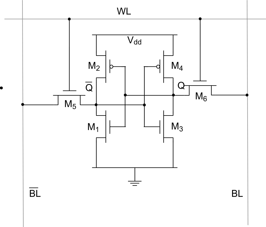
Why SRAM remembers while powered
Connect two inverters in a loop. If one node is high, it makes the other low; that low feeds back to support the first node’s high state. The opposite arrangement is also stable.
Access transistors let the read/write circuitry reach the cell. Remove its supply and the ordinary SRAM cell no longer maintains that feedback state. “Static” does not mean non-volatile.
Do all transistors act as digital switches?
No. In analog circuits, a transistor can operate around a chosen bias point, where a small input change controls a continuous current change. An amplifier converts that change into a useful output signal; its energy comes from the power supply.
For a concrete published example, Analog Devices’ common-source amplifier activity includes a circuit and input/output waveforms. It demonstrates amplification rather than binary switching. It is a manufacturer’s teaching example, not a YURUNOX laboratory test.
Why Do Transistors Consume Power and Limit Chip Speed?
An insulated gate is not an energy-free gate. It behaves partly like a tiny capacitor. Moving a signal from low to high charges capacitance in transistor gates and wiring; taking it low discharges that stored energy. Add the contributions across an active chip and the power becomes significant.
Three effects need separating: capacitive switching power, brief overlap current during transitions and leakage power even when logic is not switching. Texas Instruments separates static and dynamic contributions in its CMOS power-consumption application report.
Here, α is the average number of 0-to-1 charging events per clock cycle, C is the effective switched capacitance in farads, VDD is the supply in volts, and f is frequency in hertz. Activity-factor conventions vary; this definition counts charging events.
What does a 20% voltage reduction do to this term?
Assume α = 0.2, C = 10 pF and f = 100 MHz. At 1.0 V, the modeled capacitive switching power is 0.20 mW. At 0.8 V, with everything else fixed, it is 0.128 mW.
The ratio is 0.8² = 0.64, or 36% less for this term. That is not a prediction of 36% lower total chip power: leakage, other circuits and operating frequency can change. It is also not permission to operate below a part’s specified supply range.
Why can’t a gate change instantly?
A transistor supplies finite current to a finite capacitance. Long or heavily loaded interconnects add resistance and capacitance. A larger transistor may drive a load faster, but it also presents more capacitance to the stage before it. Designers balance these costs rather than simply making every device larger.
A chip’s useful performance also depends on architecture, memory access, software and temperature limits. More transistors can enable larger caches or more parallel work; the count alone does not guarantee that a particular task runs faster.
Why an “unused” input can still consume power
Imagine a CMOS input whose driver becomes high-impedance during reset. If no suitable bias is present, the input can float into an intermediate region. Both input-stage devices may conduct, and noise can cause unwanted switching.
TI documents these risks in Implications of Slow or Floating CMOS Inputs. The practical check is the pin’s reset state, internal bias and specified input-transition limits. Use the device’s recommended termination; there is no one pull-resistor value for every input.
How Do Planar, FinFET and Gate-All-Around Transistors Differ?
The core idea stays the same: a gate electric field controls a semiconductor channel. What changes is how effectively the gate surrounds and controls that channel as devices become smaller.

- Planar: the gate primarily controls the channel from above.
- FinFET: a raised fin lets the gate control multiple sides.
- Gate-all-around: the gate surrounds the channel, such as a nanosheet, on all sides.
Better electrostatic control helps manage leakage and switching behavior at small dimensions. The gate still acts across a dielectric; “surrounding the channel” does not mean a direct conducting connection between gate and channel. ASML’s structural comparison explains the progression.
Process-node labels are not a complete electrical specification. For a component decision, voltage limits, timing, power and temperature requirements remain more useful than assuming that one transistor shape or node name automatically makes a part better.
How Can You Tell Whether One Logic Output Can Drive Another?
Once “1” means a valid voltage range, interface selection becomes a comparison of guarantees. Check the driver’s VOH and VOL against the receiver’s VIH and VIL, under the relevant supply, load and temperature conditions.
Why Might a Nominal 3.3 V Output Still Fail the Check?
The TI SN74HC00 datasheet, section 6.3, specifies a minimum high input of 3.15 V at VCC = 4.5 V.
Now assume a separate 3.3 V driver guarantees VOH of only 2.9 V at the intended load. Its worst-case high-level margin against that receiver limit is:
2.9 V − 3.15 V = −0.25 V
That interface is not guaranteed to register a high under the stated assumptions. It does not prove that every physical board will fail. A suitable logic family or level translator may be needed after checking the complete interface.
The receiver value is from a published datasheet. The driver and load condition are hypothetical; this is not a measured customer failure or an interchangeability recommendation.
What Should You Verify Before Selecting or Sourcing an IC?
The transistor model tells you which specifications matter, but it does not approve a device. Freeze the exact orderable part number and compare guaranteed limits under the real supply, load, temperature, timing and operating-state conditions.
- Match the exact device and operating rails. Use the full manufacturer part number, package and grade. Core voltage and I/O voltage may be different; check recommended operating conditions, not only absolute maximum ratings.
- Compare guaranteed logic levels and timing. Check both high and low margins, output loading, edge-rate limits and propagation delay. A functionally similar part is not automatically electrically interchangeable.
- Include reset, idle and power-down behavior. Review unused inputs, internal pull devices, high-impedance states and power sequencing. For memory, check whether data survives the required low-power state.
- Specify power and provenance requirements separately. Use relevant active/standby conditions for the electrical review. For purchasing, identify traceability, packaging and inspection requirements; see YURUNOX’s quality-assurance information.
| Decision | Evidence to verify | Stop boundary |
|---|---|---|
| Electrical fit | Recommended operating conditions, guaranteed DC limits, timing, load and temperature | The comparison depends only on typical values, absolute maximums or an unmatched test condition |
| Functional fit | Truth table, reset and power-down states, pin behavior, memory retention and required software | An undefined, floating or unsupported state can reach the real application |
| Physical fit | Exact package code, pinout, land pattern, thermal data, moisture sensitivity and packing method | The package name looks similar but dimensions, pins or assembly controls do not match |
| Supply approval | Manufacturer status, traceability, labels, lot/date codes, storage evidence and agreed inspection or test scope | The source or evidence cannot support the buyer's risk and release requirements |
The same caution applies to discrete MOSFETs: threshold voltage alone is not a fully-on drive specification. Check the gate voltage at which the required on-resistance is specified, as explained in Toshiba’s gate-drive guidance. Do not transfer a power MOSFET’s drive voltage to a processor core.
From understanding the circuit to choosing the component
The key chain is simple: electric field → controlled current path → node voltage → logic and stored state. For a sourcing enquiry, turn that understanding into an exact part number, package, operating requirements, quantity and required delivery date.
Discuss your component requirements →YURUNOX is an electronic-component sourcing partner. Design suitability and substitution decisions require application-specific engineering review.
Sources and further reading
The explanations use simplified teaching models. Published device limits are identified separately from illustrative calculations and hypothetical scenarios. Image credits and licenses appear beside each image.
- Toshiba — What is a MOSFET?Structure, terminals and the field-effect principle.
- Toshiba — CMOS inverter operationComplementary pull-up and pull-down behavior.
- MIT Computation Structures — CMOS technologyStatic CMOS networks, NAND topology and gate behavior.
- MIT OpenCourseWare — Memory hierarchy, annotated slides6.004, Spring 2017. SRAM, DRAM and floating-gate flash teaching models.
- Analog Devices — MOS transistor common-source amplifierMay 2020. Published analog circuit activity and waveforms.
- Texas Instruments — CMOS Power Consumption and Cpd CalculationSCAA035B, June 1997. Static and dynamic power mechanisms.
- Texas Instruments — Implications of Slow or Floating CMOS InputsSCBA004E, revised July 2021. Input-transition and floating-input risks.
- Texas Instruments — SNx4HC00 datasheetSCLS181H, revised August 2021. Section 6.3 supports the 4.5 V receiver example.
- ASML — What is a gate-all-around transistor?Planar, FinFET and gate-all-around structural comparison.
- Toshiba — How much gate-source voltage should drive a MOSFET?Why a threshold specification alone does not establish adequate gate drive.