

How to Choose an Op Amp for Your Circuit
Choose an op amp by checking supply voltage, input range and loaded output swing first. Then compare DC error, noise, bandwidth, slew rate and stability under your actual circuit conditions.
A low offset number or a high MHz rating cannot rescue an amplifier that clips, loads the sensor or fails to settle. This guide turns the datasheet into a practical shortlist—and shows which details matter when buying an alternative.
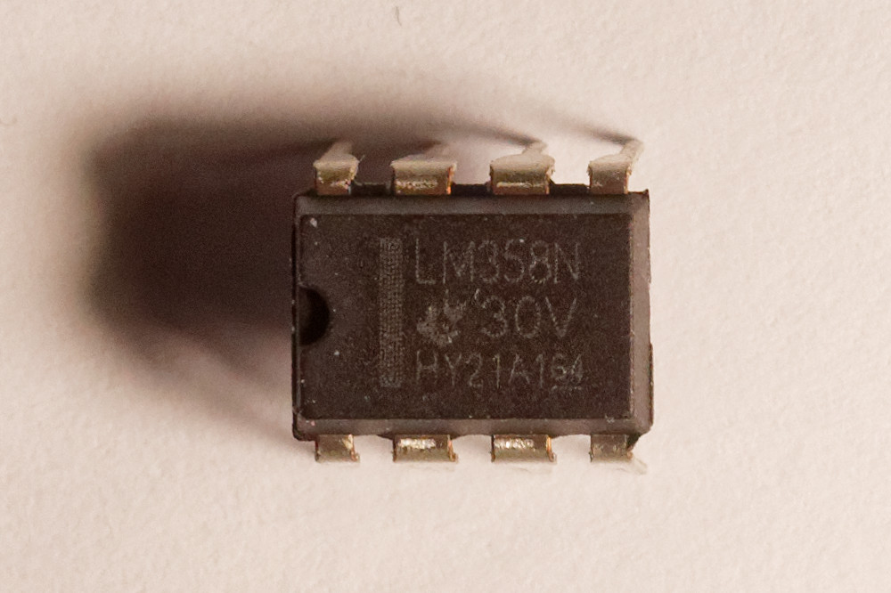
Write the circuit brief before opening a selection table
The fastest useful selection method has three stages: reject parts that cannot operate within the required voltage and temperature limits; compare the remaining parts against an error and timing budget; then validate the complete circuit, package and ordering code.
This workflow focuses on conventional voltage-feedback op amps. Current-feedback amplifiers, instrumentation amplifiers and specialized ADC drivers need their own design rules. Before comparing parts, decide whether a general-purpose op amp is the right architecture at all.
| Write down | Include these details | Why it matters |
|---|---|---|
| Supply rails | Minimum, nominal and maximum voltage; startup and power-off states. | Nominal voltage alone can hide a brownout or overvoltage problem. |
| Input signal | Range, DC level, source impedance and possible overloads. | Determines input-range, bias-current and protection checks. |
| Transfer function | Gain, polarity, reference voltage and required output range. | Sets headroom, noise gain and error amplification. |
| Timing | Highest useful frequency, peak amplitude, step size and settling time. | Small-signal bandwidth and large-signal speed are different constraints. |
| Load | Resistance, capacitance, cable length and ADC input behavior. | Changes output current, swing and stability. |
| Accuracy and environment | Allowed error, noise bandwidth, temperature, power and package. | Defines what “good enough” means across operating conditions. |
Range comes before precision. Check input and output separately.
Use the complete error budget. The smallest offset is not always the best choice.
Speed has several meanings. Bandwidth, slew rate and settling are not interchangeable.
Approve the circuit, not the label. “Rail-to-rail” and “pin-compatible” are starting points.
Check supply, input common-mode range and output swing
Read the recommended operating conditions, not just the absolute maximum ratings. Absolute maximum values are stress limits, not a promise of normal operation. For split supplies, compare the total span, V+ − V−: ±2.5 V is a 5 V total supply.
A real three-part supply screen
The following manufacturer specifications show why “precision op amp” is not a voltage specification. These parts are examples for one screening step, not a ranked shortlist or a pin-compatible substitute set.
| Example device | Recommended total supply | Supply-only decision |
|---|---|---|
| TI TLV9002 | 1.8–5.5 V | Includes 3.3 V; continue checking the circuit. |
| TI OPA197 | 4.5–36 V | Reject for operation from 3.3 V alone. |
| TI OPA388 | 2.5–5.5 V | Includes 3.3 V; continue checking the circuit. |
Source: recommended operating conditions in TLV9002 Rev. R, OPA197 Rev. C and OPA388 Rev. D datasheets. Channel count, package, input behavior and performance differ.
Rail-to-rail input and rail-to-rail output are separate claims
Input common-mode voltage is the average of the two input voltages. Negative feedback keeps them close only during normal linear operation. Check the required common-mode range against the specified limits; then check the output's linear swing at the actual sourcing or sinking current and temperature.
Rail-to-rail output does not mean zero headroom under every load. Some datasheets distinguish saturation swing from the narrower range used to specify linear performance. Rail-to-rail input stages can also behave differently around their input-pair crossover region. TI's input and output swing guide explains these distinctions.
A 3.3 V circuit with a 3.0 V output has less margin than it seems
Assume a 3.3 V supply with ±5% tolerance and a non-inverting gain of 20. An ideal 50–150 mV input produces 1–3 V. At the minimum supply of 3.135 V, the upper output has only 135 mV of rail headroom, before accounting for output error.
Selection consequence: verify linear output performance at that load and minimum rail, plus input operation at 50 mV. Passing the supply-range check does not establish either condition. If the margin is inadequate, change the gain, output range, supply or amplifier.
A single-supply circuit also needs a suitable reference if the signal would otherwise demand a negative output. A midpoint reference is not automatically a low-impedance power ground: its noise, impedance and loading enter the signal path. Check differential-input and protection limits separately during startup, overload and partial power-down.
Budget offset, bias current and drift together
Input offset voltage, VOS, appears as an input-referred error. Its approximate output contribution is noise gain × VOS. For a simple non-inverting amplifier, noise gain equals the ideal signal gain. With resistive feedback, it is 1 + RF/RG; an inverting signal gain of −1 normally has a noise gain of 2, not 1.
Use guaranteed limits at the relevant conditions when a guaranteed error budget is required. A room-temperature typical value is useful for comparison, but it is not a worst-case production limit. Include resistor ratio error, reference error and the sensor itself alongside the amplifier. See ADI's offset tutorial and input bias current tutorial.
A 50 µV offset can be smaller than the bias-current error
Assume a 100 kΩ source resistance, 10 nA input bias current, 50 µV input offset and a non-inverting gain of 20. The source-side bias contribution is 10 nA × 100 kΩ = 1 mV at the input, or 20 mV at the output. The offset contribution is only 1 mV at the output.
The useful next comparison is input bias current over temperature, not another small improvement in VOS. This simplified calculation isolates one input path; the full circuit also includes the other input's bias current and feedback resistances.
Compare two DC error contributions
For a simple non-inverting stage, enter non-negative magnitudes. Try changing the source resistance from 100 kΩ to 1 kΩ while leaving the amplifier assumptions unchanged.
- Bias contribution at output
- 20 mV
- Offset contribution at output
- 1 mV
Sum of these two magnitudes: 21 mV. This is not a complete error budget.
Bias-related input drop: 1 mV. Values shown are calculated, not measured.
Uses |IB+| × RS × noise gain and |VOS| × noise gain. Excludes the other input's bias contribution, drift, gain error, reference error, leakage, noise and clipping. Actual error signs may reinforce or cancel; do not rely on cancellation without evidence. The calculation does not approve a component.
Do not assume calibration or a balancing resistor removes everything
Initial offset calibration does not remove subsequent drift, noise or all gain error. Evaluate the temperature excursion from the calibration point, and account for whether the datasheet drift value is typical or guaranteed.
Both inputs need suitable DC return paths. A resistor added to balance input impedances can help some well-matched bias-current structures, but it can worsen error or noise in others, including some internally bias-compensated devices. Follow the exact amplifier's guidance, and control PCB leakage around high-impedance nodes.
The lowest voltage-noise number may not give the quietest circuit
Input voltage-noise density is only one contribution. Input current noise flowing through source impedance produces another voltage noise term. Resistors add thermal noise, and the feedback network determines how each contribution reaches the output.
That example shows why a device with an attractive voltage-noise specification can still be a poor match for a high-impedance sensor. Use the source's impedance across frequency—not only its DC resistance—and include both input paths where relevant.
Compare noise over the same effective bandwidth. Noise density in nV/√Hz is not the same as integrated noise in µV RMS, and RMS noise is not directly interchangeable with a peak-to-peak noise specification. For uncorrelated sources, add noise powers and take the square root; do not simply add their RMS amplitudes.
Low-frequency measurements also need the 1/f region and low-frequency noise behavior. Reducing bandwidth can reduce integrated noise, but too much filtering can prevent a switched or multiplexed signal from settling in time. The right tradeoff comes from the measurement task, not a single “low-noise” label. See ADI's noise relationships and equivalent noise bandwidth tutorial.
Use bandwidth for small signals and slew rate for large signals
Gain-bandwidth product is a first estimate, not a flatness guarantee
For a dominant-pole voltage-feedback amplifier with approximately constant noise gain, the first estimate is:
The result is approximately a −3 dB frequency, where amplitude has already fallen substantially—not the edge of a perfectly flat passband. In an ideal single-pole response, operation at one-tenth of that corner still gives about 0.5% amplitude loss. Choose margin from the allowed gain and phase error, then check the actual response. See ADI's gain and bandwidth tutorial.
Use noise gain, not automatically the absolute signal gain. Reactive feedback and source capacitance can make noise gain frequency-dependent. This simple GBW relationship should not be applied as a general rule to current-feedback amplifiers.
Slew rate depends on output amplitude as well as frequency
For a sine wave, the required maximum output slope is 2πfVPK. Use peak amplitude, not peak-to-peak amplitude.
This is a calculated requirement, not a recommended device rating. Leave margin appropriate to distortion and settling requirements, and inspect the datasheet's conditions. A typical slew rate equal to the calculation does not guarantee low distortion across units and temperature. ADI's bandwidth and flatness tutorial covers the distinction.
On a 5 V supply, centering that 2 V peak signal at 2.5 V requires an output from 0.5 to 4.5 V. It must pass the loaded swing check as well as the speed check.

Check output drive, stability and settling—not just MHz
Output short-circuit current is not a linear drive-current guarantee. Include the load and feedback network when calculating output current, and check both sourcing and sinking. A cable, filter capacitor or ADC input can make a circuit behave very differently from the datasheet's simple resistive test load.
“Unity-gain stable” does not mean stable with unlimited output capacitance. A decompensated amplifier may require a minimum noise gain. Review the load, feedback topology, recommended compensation and step response together.
AD8510: a slower response can be the useful response
ADI's published gain-of-10 AD8510 circuit with a 1 nF load compares an uncompensated response with ringing against a compensated response that is slower but monotonic. The example illustrates a tradeoff between response speed and stability, not a universal component-value recipe.
Selection consequence: ask whether the signal reaches and stays within the required error band. Do not select an alternative solely because it has a higher bandwidth. Read the original ADI article, Figures 3, 6 and 7, for the specific compensation circuit and conditions.
A series isolation resistor can help in a suitable design, but its value and placement relative to the feedback path affect bandwidth, DC error and available output swing. Use the manufacturer's analysis and validate the actual network; there is no single resistor value that makes every amplifier stable.
A slow sensor can still need a fast SAR ADC driver
A SAR ADC's switched sampling capacitor draws transient charge during acquisition. The driver and external RC network must settle before that acquisition window ends. Sensor bandwidth alone therefore cannot determine the required amplifier bandwidth.
ADS8860 example: select the amplifier and RC network together
In TI's SBAA531 example, the calculated amplifier-bandwidth requirement is above 17.8 MHz, and the design uses a 20 MHz OPA322. TI then sweeps filter resistance to compare settling responses. Those values belong to that specific ADC setup; they are not requirements for every SAR ADC.
The practical lesson is the workflow: start from resolution, input capacitance, full-scale step and acquisition time, then optimize and verify the driver plus RC network. A bandwidth check alone does not finish the design.
Illustrative troubleshooting scenario: a slow sensor reads consistently with a long acquisition time, but its code changes after shortening that time or switching from another input channel. Incomplete settling is a possibility to investigate—not a confirmed diagnosis. Check the preceding channel's step, ADC input loading and driver recovery. Simply increasing filter capacitance may make settling or stability worse.
Review zero-drift behavior, rejection and power states
Zero-drift helps DC precision, but it does not mean zero artifacts
Auto-zero and chopper techniques can reduce offset and drift. Their correction mechanisms can also create ripple, switching artifacts or intermodulation effects that matter in a wider-band or sampled system. Check the noise spectrum, input impedance interaction and filtering before choosing solely on drift. ADI discusses these issues in its zero-drift application guide.
CMRR and PSRR are frequency-dependent
Common-mode rejection ratio describes how well common-mode changes are rejected; it does not extend the permitted input range. In a discrete difference amplifier, resistor matching can limit circuit-level rejection even with an excellent op amp. Power-supply rejection also varies with frequency, so a strong DC PSRR number does not promise equal rejection at a switching regulator's ripple frequency. Check the curves and provide the recommended supply decoupling. See ADI's CMRR and PSRR tutorials.
Low quiescent current is not the whole battery calculation
Include output-load current, reference consumption, channel count, duty cycle and wake-up time. A low-current amplifier that takes too long to settle after enable may not suit a short measurement window. Check input and output behavior during shutdown, supply ramps and overload recovery, along with thermal conditions in dual or quad packages.
Which specifications matter most in your application?
All candidates must pass the operating-range checks. After that, the signal source and measurement task change the order of priorities.
| Circuit | Prioritize after range checks | Common selection mistake |
|---|---|---|
| Slow precision voltage measurement | Offset, drift, low-frequency noise and reference accuracy. | Using a typical room-temperature VOS as the entire error budget. |
| High-impedance sensor | Bias current over temperature, current noise, leakage and input capacitance. | Choosing the lowest voltage noise without checking source impedance. |
| Audio or AC signal conditioning | Integrated noise, distortion, flatness, slew rate and loaded output swing. | Checking frequency without checking signal amplitude. |
| SAR ADC driver | Acquisition settling, RC network, load stability and noise. | Matching amplifier bandwidth only to the slow sensor. |
| Battery-powered measurement | Supply range, total energy, wake-up settling and shutdown behavior. | Comparing quiescent current without the measurement duty cycle. |
| Photodiode transimpedance stage | Bias current, current noise, total input capacitance and feedback compensation. | Treating a current-to-voltage stage like a simple voltage-gain circuit. |
For a small differential signal riding on a large common-mode voltage, an instrumentation amplifier or a dedicated current-sense amplifier may simplify the design. The choice depends on range, accuracy, bandwidth and topology; a general op amp is not automatically the cheapest complete solution.
Validate the circuit, then lock the ordering code
- Make the limits explicit.
Record supply extremes, temperature, input and output ranges, load, gain, noise bandwidth and settling target. Keep minimum and maximum guarantees separate from typical curves.
- Model the complete signal path.
Include source impedance, feedback components, reference, load and ADC timing. Use the manufacturer's model, and check what it does not model: a successful simulation does not prove every protection or overload behavior.
- Measure on the intended PCB.
Check DC error, noise, clipping, ringing, settling, startup and overload recovery under relevant conditions. Keep feedback paths compact, follow decoupling guidance and configure unused channels as the manufacturer recommends.
- Document what was actually approved.
Retain the complete manufacturer part number, datasheet revision, package, pinout, channel count, temperature grade, test conditions and supporting results. Revisit affected checks when the part or circuit changes.

Same pin count is not the same component
Check the package drawing and pin assignment, not only “8-pin” or the family name. An ordering suffix can distinguish package, grade or packing options. Also verify enable pins, exposed-pad requirements and channel configuration where applicable.
Availability and incoming quality checks answer different questions from electrical suitability. A sourcing alternative still needs approval from the design owner.
Send a circuit brief with an alternative-part request
Start with the full MPN, manufacturer, package, quantity and required delivery date. If alternatives are allowed, add the supplies, gain, source impedance, input/output ranges, load, temperature, error target and timing requirements. State which parameters are mandatory and which can be negotiated.
For example: “3.3 V ±5%, non-inverting gain 20, 100 kΩ source, 50–150 mV input, 1–3 V output; load, temperature and error limits attached.” Those example values define questions to check, not approval of a particular amplifier.
Keep sourcing requirements and circuit approval connected
Discuss the complete part number and order requirements with YURUNOX. If you need an alternative, include the electrical brief so a similar package or family name does not become a substitute for engineering review.
Op amp selection FAQs
What should I check first when choosing an op amp?
Check the recommended supply range, input common-mode range and loaded output swing across your operating conditions. A device that fails these checks cannot be rescued by a better noise or offset specification.
Is a rail-to-rail op amp always the best choice?
No. Rail-to-rail input and output can help on low-voltage supplies, but they are separate features with device-specific limits. Check headroom under load, input behavior, noise, distortion and power against your circuit requirements.
How much gain-bandwidth product do I need?
For a suitable dominant-pole voltage-feedback amplifier, estimate closed-loop bandwidth as GBW divided by noise gain. Then allow margin for your permitted amplitude and phase error and verify the real response. There is no universal multiplier that approves every circuit.
What is the difference between bandwidth and slew rate?
Bandwidth describes small-signal frequency response. Slew rate limits how quickly the output voltage can change during a large signal. A sine wave requires a maximum slope of 2π times frequency times peak output amplitude; both checks are necessary.
Should I choose the op amp with the lowest voltage noise?
Not automatically. Current noise through source impedance, resistor noise, feedback gain and effective bandwidth can dominate the total. Compare integrated circuit noise under the same conditions, especially with high-impedance sensors.
Can a unity-gain-stable op amp drive any capacitive load?
No. Output capacitance can reduce phase margin and cause ringing or oscillation. Check the specific load, feedback arrangement and manufacturer guidance, then verify stability and settling with the complete circuit.
Can I use an op amp as a comparator?
Do not assume so. Op amps are generally intended for closed-loop linear operation, while comparator service involves large differential inputs and output saturation. Check explicit manufacturer guidance, input protection, recovery behavior and output compatibility, or select a comparator.
Is a faster pin-compatible op amp a safe replacement?
Not by itself. Higher bandwidth can change stability, noise and sensitivity to PCB parasitics. Recheck supply and signal ranges, bias current, load, minimum stable gain, power states and the complete ordering code before approving a replacement.
Technical sources and example boundaries
The calculations in this guide use stated illustrative assumptions. The AD8510 and ADS8860 discussions summarize published manufacturer examples, not YURUNOX measurements or customer projects. Use current manufacturer specifications for the exact device and conditions being approved.
- Texas Instruments: Op Amp Input and Output Swing Limitations, SBOA583—common-mode range, load-dependent output swing and linearity.
- Texas Instruments datasheets: TLV9002, OPA197 and OPA388—recommended supply ranges in the comparison.
- Analog Devices: MT-037, Input Offset Voltage and MT-038, Input Bias Current—DC error mechanisms and bias-current considerations.
- Analog Devices: MT-033, Voltage Feedback Op Amp Gain and Bandwidth and MT-045, Bandwidth and Bandwidth Flatness—noise gain, small-signal response and large-signal limits.
- Analog Devices: Practical Techniques to Avoid Instability Due to Capacitive Loading—published AD8510 compensation example.
- Texas Instruments: SBAA531, Selecting the Amplifier and Optimizing the RC Circuit and Worst-Case Settling—ADC driver selection and verification.
- Analog Devices: How to Use Zero-Drift Amplifiers in Wider Bandwidth Applications—correction artifacts and filtering considerations.
- Analog Devices: MT-042, Common-Mode Rejection Ratio and MT-043, Power Supply Rejection Ratio—rejection versus frequency.
- Analog Devices: Using Op Amps as Comparators—limitations of open-loop comparator use.