

How to Read an IC Datasheet Before You Approve a Part
Read an IC datasheet by starting with your circuit limits, not page one. Confirm the exact manufacturer part number and package; reject candidates outside recommended operating conditions; then read electrical and timing limits with their test conditions and footnotes. Before approval, verify startup, layout, thermal, ordering and errata information, and record every unresolved gap.
The useful result is not a highlighted PDF. It is a reviewable evidence record showing why the exact IC fits the intended circuit, which assumptions still need testing, and what prevents engineering or purchasing release.

What Should You Define Before Reading an IC Datasheet?
An IC datasheet connects the device's function to its permitted conditions and specified performance. Start with your circuit requirements. Then make three passes: screen the candidate, integrate it, and document the release decision.
Before opening the PDF, list the actual supply range, input range, output load, ambient temperature and required response time. Add startup, shutdown and the case where a neighboring device remains powered. These conditions tell you which rows deserve attention.
Keep the manufacturer's PDF open while reading this guide. Search for section names rather than fixed page numbers: document layouts and revisions change.
Which Datasheet Section Should You Read for Each Design Risk?
Use this map to find the first controlling evidence and the condition that prevents approval. The front page is useful for screening; detailed tables, notes, drawings and related documents decide whether the headline applies to the exact circuit.
Scroll sideways to compare every decision column →
| Condition or question | Read first | Evidence to record | Stop boundary |
|---|---|---|---|
| Exact variant or package is unclear | Device information, pin functions, package drawing, ordering information | Manufacturer, complete MPN, package code, pin view, document revision | Stop until the exact physical and electrical variant is identified |
| Supply, temperature, or pin stress may be close to a limit | Absolute maximum ratings, recommended conditions, electrical characteristics | Rail tolerance, ripple, transients, sequencing, load, temperature, applicable notes | Stop if the normal operating envelope or required margin is not demonstrated |
| Two devices must exchange analog or digital signals | Pin functions, input/output limits, timing tables, measurement conditions | Driver guarantees, receiver requirements, load, units, temperature, noise and timing margins | Stop if either end relies on a typical value or an incompatible condition |
| Startup, reset, fault, or configuration behavior matters | Functional description, register defaults, timing, application notes, errata | Power sequence, reset state, required delay/status, recovery action, validation owner | Stop if an undefined or unhandled state can violate the product requirement |
| PCB footprint, heat, or assembly may control success | Mechanical drawings, land pattern, layout guidance, thermal information | Package view, dimensions, exposed pad, board assumptions, dissipation, airflow | Stop if the approved footprint or thermal boundary does not match the exact package and board |
| The part is being released or substituted | Ordering information, revision history, current errata, lifecycle and change documents | Exact order code, approved alternate status, document set, open issues and responsible approver | Stop purchasing release when identity, applicability, or engineering approval remains unresolved |
For a detailed manufacturer explanation of this structure, see TI's Understanding and Interpreting Standard-Logic Data Sheets. Its scope is standard logic; the selected IC's own document controls.
How Do You Confirm the Exact Device, Variant, and Package?
A shortened family name is not a purchasing specification. Start at the manufacturer's official documentation and verify the complete device variant, temperature grade and package. Record the PDF revision; do not combine one variant's speed with another variant's voltage range.
If a distributor listing disagrees with the PDF, resolve the discrepancy before using either number. It may describe a different suffix, package or revision. The block diagram also matters: a feature marked “reference” may still require an external source.

Read the view before the numbers
Identify top view versus bottom view, locate pin 1, and match the drawing to the footprint. Mark supply, ground, inputs, outputs and any exposed pad. Read the pin-function table, not only the drawing.
An active-low signal, an open-drain output and a reserved pin each imply different connection rules. Do not assume that every unused input, NC pin or exposed pad should be treated alike.
One buffer function does not mean one pin map
In TI's SN74LVC1G17 pin table, VCC is pin 5 for DBV/DCK/DRL/DPW packages, pin 6 for DRY/DSF, and ball A2 for YZP/YZV. The correct function with the wrong footprint is still the wrong part.
Source: SN74LVC1G17, Rev. Y, pin configuration and functions.
What Is the Difference Between Absolute Maximum and Recommended Operating Conditions?
Absolute maximum ratings describe stress boundaries. Recommended operating conditions define the intended operating envelope. Electrical tables then specify performance under their stated conditions. These three questions must remain separate.
The 6 V proposal does not become acceptable because it is below 7 V. Change the supply or evaluate a device specified for that operating point. TI TLV320x, Rev. C, sections 6.1 and 6.3.
Calculate voltage at the IC pins, including tolerance. An illustrative 3.3 V rail with ±5% tolerance spans 3.135–3.465 V before additional ripple, startup overshoot or wiring drop. Include those separately in the power budget.
Also read the stress-table notes. A set of individual maxima does not necessarily permit all maxima at once. Input current, pin voltage and junction temperature can impose interacting restrictions.
How Should You Read Minimum, Typical, and Maximum Values?
Read a specification as one complete sentence: this parameter has this value, for this device, under these conditions. Begin with the text above the table; an individual row can override those default conditions.
Scroll sideways to compare conditions and limits →
| Parameter | Condition | Min | Typ | Max | Unit |
|---|---|---|---|---|---|
| Quiescent current, IQ | TA = 25°C | — | 40 | 50 | µA |
| Quiescent current, IQ | TA = −40 to 125°C | — | — | 65 | µA |
- Locate the quantity and unit.IQ is quiescent supply current. Microamps and milliamps differ by a factor of 1,000.
- Keep the supply and temperature attached.The 5 V table contains different limits for 25°C and the wider temperature range.
- Choose the relevant column.40 µA is typical; it is not the maximum-current budget. A dash supplies no numerical bound.
- Read the notes and definition.Quiescent current is not a complete system power calculation. Output loading and the rest of the circuit need their own accounting.
Source: TLV320x Rev. C, electrical characteristics at VCC = 5 V.
Typical is useful, but not a worst-case promise
A typical value helps explain representative behavior. For a requirement needing a defined boundary, find the applicable minimum or maximum and its qualifications. A blank cell does not mean zero; a prototype measurement does not create a manufacturer guarantee for future units. ADI explains typical values and testing conditions.
Footnotes can change the conclusion. In the MAX1358B datasheet, Note 2 identifies specifications guaranteed by design or characterization. Note 7 identifies specifications that are not production tested or guaranteed. “Not production tested” alone therefore does not settle guarantee status. Read the attached notes on page 10.
How Do You Check Logic-Level and Signal Compatibility?
A receiver's input-high threshold tells you what it needs. A driver's output-high limit tells you what it can provide at a specified load. Compare the relevant limits, not just two “3.3 V” labels.
Check both high and low noise margins
Assume the driver guarantees VOH(min) = 2.4 V and VOL(max) = 0.2 V at the intended load. The receiver requires VIH(min) = 2.0 V and permits VIL(max) = 0.8 V.
High margin = 2.4 − 2.0 = 0.4 V
Low margin = 0.8 − 0.2 = 0.6 V
These positive static margins do not establish timing, transient immunity or power-off compatibility. Supply and temperature conditions must match, and ground differences consume margin.
For an analog connection, distinguish input range, common-mode range, differential range and output swing. A voltage can satisfy one of those limits while violating another. Open-drain or open-collector outputs also require a suitable pull-up or load to establish high.
How Do You Build a Complete Timing Budget?
Timing requirements describe what the IC needs at its inputs: setup time, hold time and pulse width, for example. Switching characteristics describe its response. Read the waveform diagram to identify the starting edge, ending edge and voltage crossing used for each interval.
Read past the “40 ns” headline
The TLV3201 switching table gives 47 ns typical low-to-high delay at 5 V, 20 mV input overdrive and 15 pF load. Overdrive is the amount beyond the comparison threshold in the test. A required maximum response time cannot be approved from that typical value or the front-page headline.
Build the complete path: upstream delay, interconnect effects where relevant, the IC's response, and the receiving device's requirements. Preserve any unbounded item as an open issue instead of silently substituting a typical number.
Use curves to investigate, not to invent guarantees
Read both axes, units, scale and curve labels before drawing a conclusion. Ask which conditions remain fixed. A typical current-versus-temperature plot can flag the hot corner for investigation, but it is not automatically a production limit. Avoid extrapolating beyond the plotted range.
If a bench result differs, reproduce the documented supply, signal, load and mode as closely as practical. Include the probe's capacitance and measurement uncertainty before deciding the part is out of specification.
Why Does the ADS1115 ±6.144 V Range Not Permit a 6 V Input?
The ADS1115 analog-to-digital converter offers a ±6.144 V full-scale setting. Its recommended voltage at each analog input is nevertheless GND to VDD. On a 3.3 V supply, selecting that scale does not allow a 6 V input.
The separate analog-input stress range is GND − 0.3 V to VDD + 0.3 V. That is not an extension of the normal measurement range. Source: ADS111x Rev. E, sections 5.1 and 5.3.
A 0–6 V sensor meets a 3.3 V ADC
A buyer sees “±6.144 V” and assumes direct connection is possible. The review instead flags an input-interface redesign. An attenuator or other front end needs checks for tolerance, ADC loading, settling, faults and power sequencing. The range register alone cannot solve the mismatch.
For differential measurements, write down both input-to-ground voltages as well as their difference. For example, inputs at 1.0 V and 2.0 V have a −1.0 V difference without either pin being below ground. The selected scale and all other conditions must still be suitable.
What Startup, Reset, and Default-State Behavior Must You Verify?
Read reset behavior, enable polarity, startup time, default mode, fault response and register access rules. A typical application drawing rarely explains all of them. Reserved bits and write-one-to-clear fields need the device-specific instructions.
The ADS111x enters power-down after reset: the interface remains active, but conversions are not running. This is a documented startup state, not evidence of a failed ADC. See Rev. E, section 7.4.
Turn the functional description into a sequence: establish valid rails, release reset as specified, configure the device, confirm readiness and use the output. For each step, record the actual condition or status indication. A delay that happened to work once is not a defined startup requirement.
What Layout, Thermal, and Package Details Affect the Real Design?
Application circuits are starting points with assumptions. Compare their supply, load, external components and operating mode with your design. Turn layout advice into specific checks: the decoupling capacitor beside its pin, the sensitive input away from a switching node, and the return path that completes the current loop.
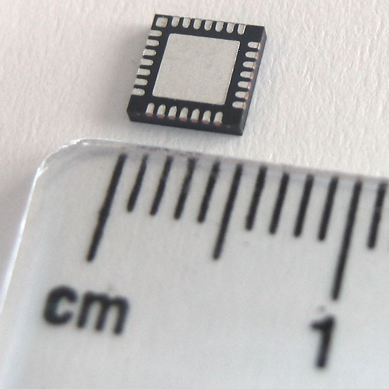
Body size is only one dimension
Check lead pitch, height, pad or ball arrangement, exposed-pad requirements and the drawing's view. Confirm the manufacturer package code against the approved footprint and assembly process.
The complete ordering code can also distinguish grade and packing options. A purchasing substitution therefore needs more than matching the family name and body dimensions.
A thermal number needs a board and an environment
Ambient, case and junction temperatures refer to different locations. Junction-to-ambient thermal resistance, θJA, depends on board construction and environment; it is not a universal temperature-rise constant for every PCB. TI's Semiconductor and IC Package Thermal Metrics explains this limitation.
For a thermally important part, retain dissipation, package, copper, airflow and temperature-limit assumptions. Use an appropriate thermal model and validation plan instead of approving the design from the ambient operating range alone.
Likewise, component human-body model and charged-device model ESD ratings do not establish finished-product IEC 61000-4-2 immunity. Connector protection and system testing require their own assessment. TI explains the component/system ESD distinction.
Which Datasheet Revision and Errata Apply to the Exact IC?
A microcontroller may need a datasheet, reference manual and errata sheet together. The datasheet covers ratings and interfaces; the manual explains operation; errata identifies known limitations or corrections. Their revision identifiers do not necessarily move together.
Applicability comes before the workaround
ST's ES0334 lists affected STM32F76xxx/77xxx products and silicon revision codes, then describes limitations and workarounds. First confirm the exact product and silicon revision; then determine whether the affected function is used. The STM32F103 in the opening photo is a different family.
Source: STMicroelectronics ES0334, applicability tables and limitation sections.
Record the relevant erratum, design impact, required action and verification owner. If official documents conflict, request clarification. Do not resolve the conflict by selecting whichever statement makes the proposed circuit look acceptable.
What Evidence Should You Record Before Releasing the Part?
A useful entry records the requirement, document revision, section or row, applicable conditions and remaining gap. “Supports 3.3 V” is incomplete. “Supply checked against 3.135–3.465 V; startup overshoot unresolved” tells the next reviewer what to do.
Scroll sideways to review the example evidence record →
| Requirement | Evidence recorded | Remaining action |
|---|---|---|
| Supply compatibility | Operating range; rail-tolerance calculation | Measure or bound startup and ripple |
| 0–6 V sensor input | ADS1115 per-pin range at the selected supply | Design and validate the input interface |
| Response-time budget | Delay row, supply, overdrive and load | Resolve any typical-only contribution |
| Board and firmware fit | Package map, startup sequence, applicable errata | Verify footprint and relevant workarounds |
Use This Reading Checklist Beside the PDF
Mark a topic only after recording its evidence and open issues. This is a reading aid, not engineering approval. Selections stay in this page session only and are not sent anywhere.
0 of 8 topics marked reviewed. Open issues still need a documented disposition.
What Information Should Procurement Include in the IC Enquiry?
Engineering approval and commercial availability are separate checks. An available substitute still needs the same electrical, physical and startup review. State whether an alternative is already approved or is only being proposed for evaluation.
Planning delivery after the technical review? See YURUNOX's global shipment information.
Which Manufacturer Documents Support This Reading Method?
These documents support the reading examples. Follow the current official documentation for the exact device and revision you plan to use.
- TI SZZA036C: Understanding and Interpreting Standard-Logic Data Sheets — section meanings and interpretation.
- TI TLV320x datasheet, Rev. C — supply limits, current and switching conditions.
- TI ADS111x datasheet, Rev. E — input scaling, per-pin limits and startup.
- TI SN74LVC1G17 datasheet, Rev. Y — package-specific pin functions.
- ADI: Typically Testing “Typical” in a Typical Manner — statistical values and conditions.
- ADI MAX1358B datasheet — testing and guarantee qualifications.
- TI SPRA953: Semiconductor and IC Package Thermal Metrics — thermal-metric limitations.
- TI SSZTBK1: Protecting Industrial Human-Machine Interfaces — component versus system ESD.
- ST ES0334: STM32F76xxx/77xxx Device Errata — product and silicon-revision applicability.
Product examples explain documentation; they are not part recommendations, YURUNOX test reports or customer outcome claims. Illustrative calculations do not replace application-specific analysis and validation.