

Micron Memory x4 vs x8 vs x16 Explained
x4, x8, and x16 state how many DQ data bits one DRAM component transfers in parallel. They do not state total capacity or make one option automatically faster. Choose the width from the controller rules, required bus and ECC organization, rank capacity, bank behavior, package count, layout, and exact Micron orderable part.
A simple 64-bit data rank uses sixteen x4, eight x8, or four x16 components. At the same component density, those ranks hold different capacities; at the same transfer rate, their ideal 64-bit bus bandwidth is equal.
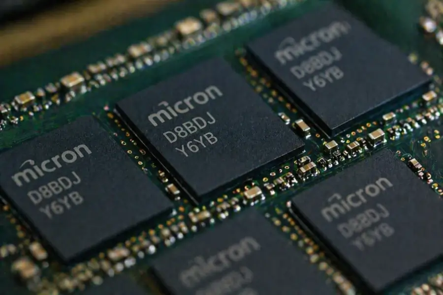
The right width is the one the complete memory interface supports
The controller reference design and population rules outrank a catalog shortcut.
x4, x8, and x16 devices required, before any sideband ECC devices.
Equal transfer rate and assembled bus width give equal ideal bus bandwidth.
Width never replaces the complete orderable code and its current documentation.
There is no universal winner. x4 can support high capacity per rank and finer device-fault granularity in server architectures that are designed for it, but it raises package count and shared-net loading. x16 can cut package count in supported embedded interfaces, but it may reduce bank resources and fail a simple sideband-ECC mapping. x8 is often the middle ground, yet it is still only correct when the controller, package, topology, and capacity arithmetic agree.
x4, x8, and x16 describe one component's external data width
A DRAM component contains a much larger internal bit array than it exposes on its package. The x-organization states the number of DQ pins that carry data for that one component: four for x4, eight for x8, and sixteen for x16. Address, command, clock, reset, power, reference, and strobe signals are separate from this count.
Micron catalogs list component density and component configuration as different fields. A 16Gb component can be described conceptually as 4G × 4, 2G × 8, or 1G × 16. Each organization stores 16 gigabits, but it exposes a different number of data bits per addressed location.

Do not confuse Gb, GB, x-width, and rank count
A component catalog normally expresses device density in gigabits (Gb), while module and system capacity is normally expressed in gigabytes (GB). Eight bits make one byte. A 16Gb component therefore contains 2GB of raw bit capacity, but a rank contains multiple components.
The label 1Rx8 does not mean one x8 chip or an 8GB module. It means one independently selected rank assembled from x8-organized DRAM devices. Physical package placement on one or two PCB sides does not determine rank count.
| Field | Component-level meaning | Module or system-level meaning |
|---|---|---|
| x4 / x8 / x16 | DQ bits exposed by one DRAM component. | Changes component count, supported topology, capacity granularity, and organization-specific behavior. |
| x64 / x72 / x80 | Not a normal width for one standard DDR component. | Aggregate data-plus-check-bit width of a module or memory interface. |
| 1R / 2R / 4R | Not the device width. | Number of independently selected ranks. |
| 16Gb / 24Gb / 32Gb | Stored bits in one component when used in a component catalog. | Multiply by the applicable component or die count before converting to bytes. |
| 16GB / 32GB / 64GB | Unusual as the label for one monolithic DDR component. | Nominal module or usable system capacity in bytes. |
The bus width determines device count; density determines capacity
A rank is a group of DRAM components selected together to present the data width expected by the controller. In an ideal 64-bit data-rank example, device count is the rank data width divided by component width.
With monolithic 16Gb components, the x4 rank contains 16 × 16Gb = 256Gb = 32GB. The x8 rank contains 8 × 16Gb = 128Gb = 16GB. The x16 rank contains 4 × 16Gb = 64Gb = 8GB. Narrower devices produce more capacity per rank at equal device density because more components are needed to fill the same bus.
| Organization | Data devices | Usable capacity | What changes |
|---|---|---|---|
| 16Gb x4 | 16 | 32GB | Highest package count and capacity per rank in this equal-density example. |
| 16Gb x8 | 8 | 16GB | Middle package count and capacity granularity. |
| 16Gb x16 | 4 | 8GB | Lowest package count and capacity per rank in this example. |
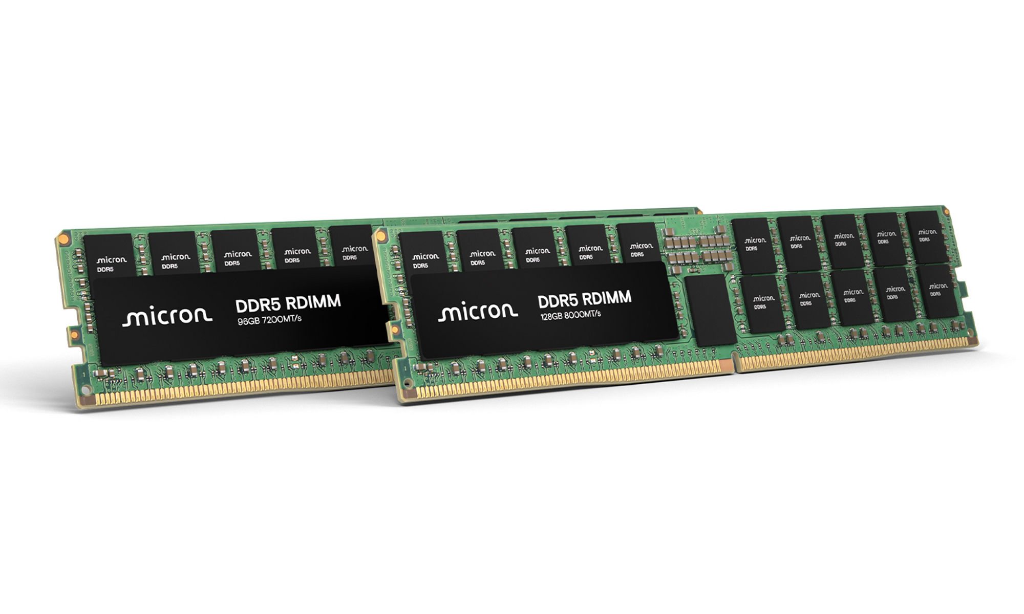
DRAM rank and bandwidth calculator
Model a simple interface built from identical devices. The calculation separates usable data width from optional sideband-ECC bits and flags combinations that do not divide evenly.
- Data devices / rank
- 8
- Total devices / rank
- 8
- Usable capacity / rank
- 16.00 GB
- Ideal data bandwidth
- 25.60 GB/s
One rank provides 16.00 GB usable capacity in this simple model. Validate the exact controller, device, topology, and ECC implementation.
x16 has more bandwidth per package, not automatically more system bandwidth
At 3200 MT/s, one x4 component moves 1.6 GB/s of ideal data, one x8 component moves 3.2 GB/s, and one x16 component moves 6.4 GB/s. That per-package comparison is incomplete because the controller selects enough components in parallel to build its required bus.
Sixteen devices work in parallel for a 64-bit data rank.
Eight devices work in parallel for the same 64-bit data width.
Four devices work in parallel for the same 25.6 GB/s ideal rank-level result.
Real sustained performance can still differ. Page size, bank count, bank groups, partial-write behavior, refresh, rank interleaving, command scheduling, access locality, controller policy, and signal-integrity margin affect useful throughput. The correct claim is therefore: equal data width and transfer rate give equal ideal peak bandwidth, while organization can change how efficiently a specific controller and workload reach it.
x4 can improve device-fault granularity, but the controller creates the correction capability
A traditional 64-bit data path plus eight sideband check bits forms a 72-bit path. In a simple design using identical components, 72 divides into eighteen x4 devices or nine x8 devices. It does not divide evenly into x16 devices. That arithmetic explains why x4 and x8 are common in sideband-ECC modules, but it does not prove that every controller supports either organization.
| ECC term | What it protects | How x4/x8/x16 matters |
|---|---|---|
| DDR5 on-die ECC | Internal array operations inside each DDR5 device. | A device-level DDR5 feature; it does not create an external x72 module bus. |
| Sideband ECC | Controller-visible data plus dedicated check-bit lanes. | The total bus width must map to a controller-supported component organization. |
| Device-fault correction | Multiple errors confined to one physical DRAM device, when the platform algorithm supports it. | A narrower device contributes fewer bits to a codeword, but controller code and physical mapping decide what is correctable. |
| Inline ECC | Controller-managed check data stored in normal memory resources. | Can support a different component mix than sideband ECC, but consumes capacity or bandwidth and remains platform-specific. |
On-die ECC is not the same as an ECC DIMM
Micron's DDR5 architecture white paper describes 128b+8b single-error correction inside the device, with error check and scrub. That strengthens the internal array, but it does not protect every fault on the package pins, PCB traces, connectors, or controller path.
A system may use DDR5 on-die ECC together with sideband or inline ECC. Treat them as layers with different visibility, coverage, telemetry, and qualification evidence.
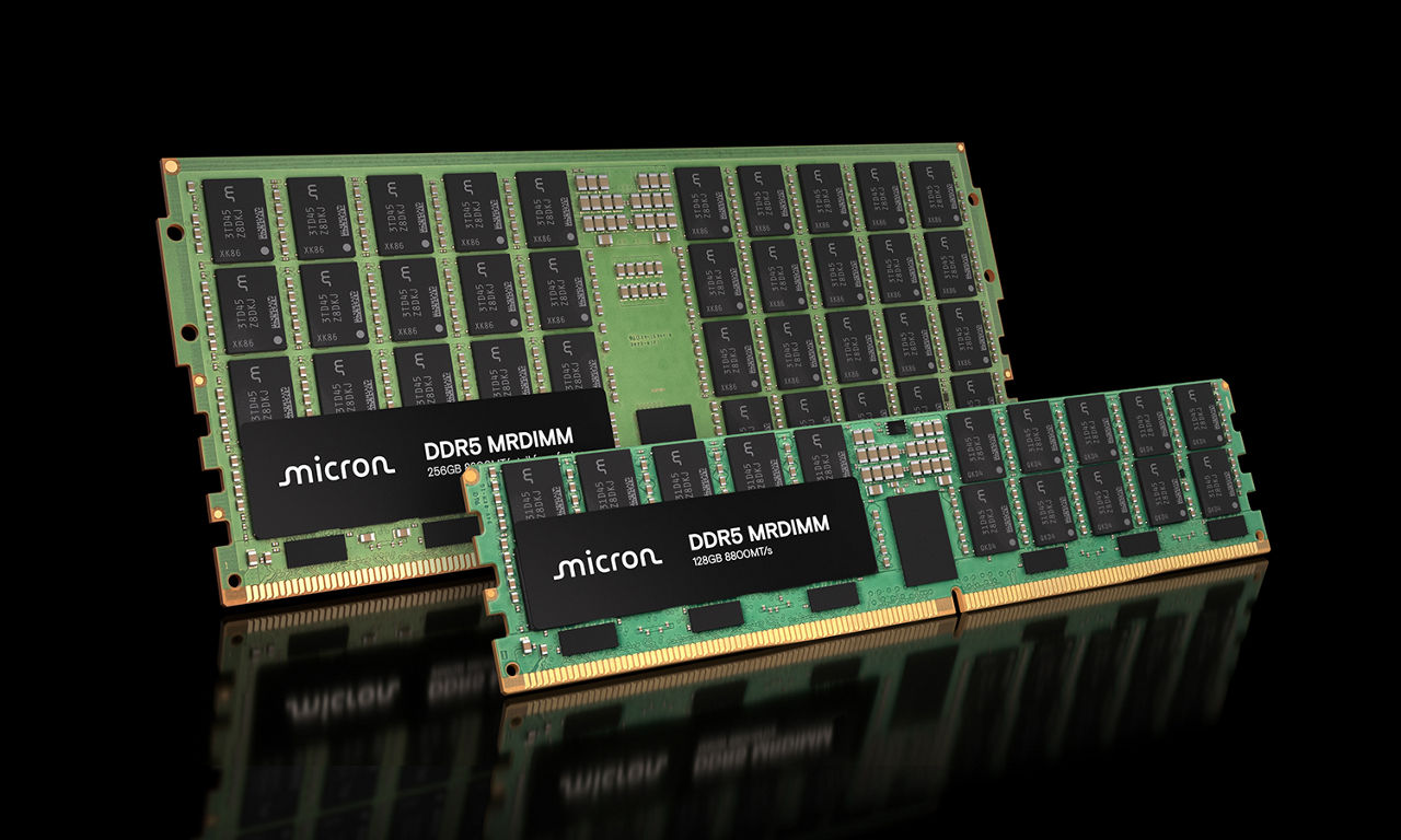
The width labels persist from DDR4 to DDR5, but the surrounding architecture changes
x4, x8, and x16 continue to mean DQ bits per component, but DDR4 and DDR5 do not organize or train the complete interface in the same way. Micron's current DDR5 material lists higher data rates, 16n prefetch, more mode-register space, expanded training functions, on-die ECC, read/write CRC, and different bank structures from DDR4.
For 16Gb to 64Gb DDR5 devices, Micron's public comparison lists eight bank groups with four banks each for x4/x8, versus four bank groups with four banks each for x16. Its DDR4 comparison lists four groups of four banks for x4/x8 and two groups of four banks for x16. These are architecture-specific facts, not a reason to assume every x8 is faster than every x16.
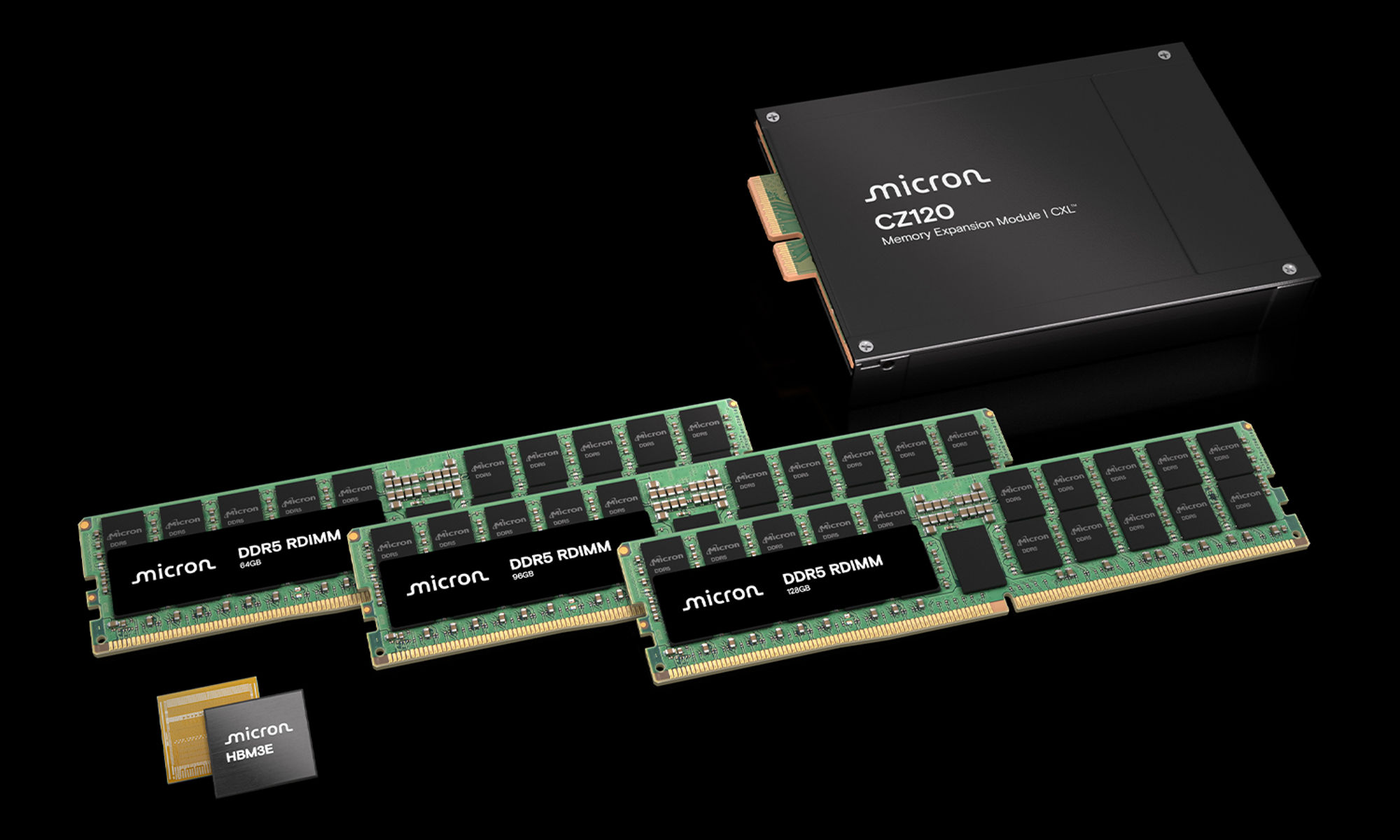
Module width is another layer
Micron's DRAM Module Quick Reference Guide lists module bus widths such as x64, x72, and x80 across form factors and generations. Those figures describe the aggregate module interface, not one DRAM package.
DDR5 DIMMs also divide the module data path into subchannels. A module-level x80 label can still be implemented with x4 or x8 devices according to the registered-module architecture. Read component organization, module width, rank count, and subchannel behavior as separate fields.
| Area | Why it matters | Evidence to review |
|---|---|---|
| Banks and page behavior | Organization can change conflicts, locality, partial writes, and scheduling opportunity. | Exact-device data sheet and controller performance guidance. |
| DQ/DQS and mask signals | Lane grouping and data-mask or DBI support affect pin mapping and writes. | Package ballout, controller pinout, and reference schematic. |
| Training and timing | Higher rates depend on supported training, mode registers, and timing bins. | Controller configuration, Micron speed-grade data, and training logs. |
| Module subchannels | DDR5 module-level paths cannot be interpreted as one DDR4-style wide channel. | Module data sheet, SPD, platform guide, and population rules. |
| Reliability functions | On-die ECC, CRC, parity, sideband ECC, and inline ECC cover different faults. | Device, module, controller, firmware, and RAS documentation. |
Published controller and catalog examples show where simple width rules fail
The following situations are public manufacturer evidence or clearly labeled architectural examples. They are not YURUNOX customer projects, independent benchmarks, hardware test results, or proof that a specific Micron device is approved for a finished system.
16Gb DDR5 at 5600: x16 exposes fewer bank resources
AMD's DDR5 Component Choice table is explicitly limited to 16Gb devices at the 5600 speed grade. It lists 32 banks and eight bank groups for x4 and x8, versus 16 banks and four groups for x16. It also lists no data mask for x4 in that example and different tFAW values.
Decision consequence: a workload with random or multi-thread traffic may respond differently from a streaming workload. Use the table as controller-specific evidence, not a universal x4/x8 ranking.
A valid width can still be invalid with sideband ECC
AMD's Memory Configuration Support lists component-width rules by configured data path and states that sideband ECC is not supported with x16 components in the documented component interface.
Decision consequence: do not add eight check bits to an x16 shortlist after the schematic is complete. ECC mode and supported component width must be chosen together at architecture definition.
Same generation and density do not imply the same lifecycle
On August 28, 2026, Micron's public DDR5 part catalog showed 16Gb entries across x4, x8, and x16 with mixed status codes, including Production, Contact Sales, and End of Life. Status varies by complete orderable part, not just width.
Decision consequence: freeze the exact MPN and recheck current status before design release or purchase. This dated catalog snapshot is not a promise of future availability.
Two x16 packages can meet a 32-bit bus, but only if the controller supports them
With 16Gb devices, two x16 components provide a 32-bit data path and 4GB usable capacity in a simple one-rank model. Four x8 devices would provide 8GB, while eight x4 devices would provide 16GB at the same device density.
Decision consequence: x16 can reduce placement and package count, but capacity target, bank behavior, sideband ECC, ballout, routing, controller training, and lifecycle may change the result.
Package count changes routing, loading, power distribution, and validation work
For a fixed controller data width, narrower components require more packages. That adds power and ground connections, decoupling sites, DQ/DQS groups, placement constraints, and shared command/address/clock loads. Wider components reduce package count but place more data lanes in one package and can require a different BGA, ballout, byte-lane rule, or calibration mode.
DQ and DQS are grouped
Match the controller's byte or nibble lanes, strobe pairing, data mask/DBI, swaps, and calibration rules for the exact organization.
More devices add loads
Command, address, clock, reset, chip-select, and ODT topologies must be simulated with the production-intent package and PCB.
Package count is not power
Use exact device currents or power models, activity assumptions, refresh, termination, voltage, and thermal environment.
What to model before layout release
- Production controller package, Micron device model, topology, stackup, trace geometry, vias, termination, and connectors.
- DQ/DQS skew and eye margin by lane, plus command/address/clock timing and loading across voltage and temperature.
- Power-rail impedance, VREF behavior, decoupling placement, simultaneous switching, refresh, and worst-case activity.
- One-rank versus multi-rank loading, supported population rate, training results, and controller-specific derating.
- Package dimensions, keepouts, escape routing, assembly constraints, reflow, moisture sensitivity, and inspection access.
Use x4, x8, or x16 only after the controller and capacity math agree
| Decision question | x4 | x8 | x16 |
|---|---|---|---|
| DQ bits per component | 4 | 8 | 16 |
| Devices for 64-bit data rank | 16 | 8 | 4 |
| Simple 72-bit sideband-ECC mapping | 18 devices | 9 devices | Does not divide evenly |
| Common strength | High capacity per rank at equal density; finer device-fault granularity when supported. | Balanced package count, capacity, routing, and broad use. | Fewest packages for a fixed data width. |
| Common burden | Highest package count, placement, shared-net loading, and routing work. | Middle-ground tradeoffs still require exact controller support. | Lower capacity per rank at equal density; sideband-ECC and bank restrictions may apply. |
| Good starting context | Server or RAS design explicitly built around x4. | General DIMM or discrete design with strong x8 reference support. | Compact embedded interface where x16 is explicitly allowed. |
RAS or capacity per rank drives
The controller and reference design support x4, the ECC organization uses x4 granularity, and the board can absorb the package and routing burden.
The middle ground is qualified
Capacity maps cleanly, package count is manageable, sideband ECC is supported when needed, and controller documentation is strongest for x8.
Low package count matters
The controller explicitly supports x16, the target capacity is modest, sideband ECC is unnecessary or specially supported, and bank behavior fits the workload.
Server DIMM with chip-fault containment requirement
Start from the processor's qualified module types and RAS documentation. If the platform correction scheme is built around x4 devices, an x8 module with the same capacity and speed is not an automatic alternate.
Approval evidence: platform AVL, module MPN, rank and component organization, SPD, firmware support, error-injection or RAS validation where applicable, and lifecycle.
Embedded controller with 32-bit discrete DDR5 interface
Two x16 devices may minimize packages, but four x8 devices can double usable capacity at equal device density. The controller may expose different ECC, pinout, or width options.
Approval evidence: controller IP configuration, reference schematic, package ballout, SI/PI model, data-sheet timing, training logs, and thermal-corner test.
A selection sequence that prevents late redesign
- Lock the controller configuration. Record DDR generation, data width, ECC mode, supported component widths, densities, ranks, packages, and population-rate limits.
- Calculate usable capacity. Keep device density in Gb, system capacity in GB, component count, rank count, and any reserved ECC capacity separate.
- Screen organization behavior. Compare banks, bank groups, page size, mask/DBI, burst, refresh, timings, and workload implications for the exact speed grade.
- Resolve the package and topology. Match ballout, DQ/DQS groupings, command/address/clock loads, power rails, VREF, ODT, reset, and training.
- Freeze the exact Micron MPN. Verify temperature, qualification, die or revision constraints, status, packing, and change-control needs.
- Validate hardware at the corners. Review training margins, memory tests, ECC behavior, thermal and voltage corners, worst-case traffic, and production-intent PCB conditions.
A catalog match is a candidate, not proof of interchangeability
Micron's DRAM cross-reference tool allows filtering by technology, density, width, package, data rate, temperature, and automotive status. The same page states that Micron makes no representation about accuracy, equivalency, interchangeability, or suitability and instructs users to consult the Micron data sheet.
That boundary is important for alternate-part control. A result with matching DDR generation, density, x-width, and speed can still differ in package ballout, supported timing, refresh behavior, operating temperature, qualification, die revision, lifecycle, or controller validation.
Read the complete orderable code and status
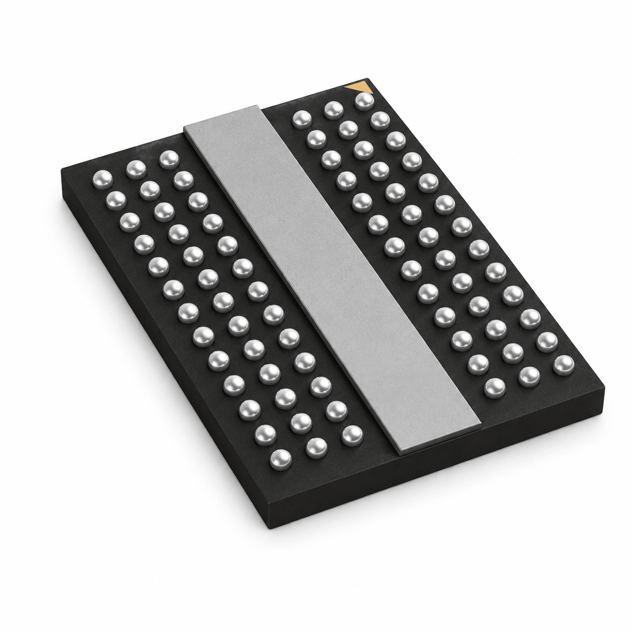
The YURUNOX Micron page uses the x8 DDR4 component MT40A1G8SA-075:E as a concrete sourcing direction. Even when a base family appears familiar, approval still needs density, x8 organization, speed suffix, 78-ball package, temperature grade, revision, controller support, and current status.
Micron's current DDR4 and DDR5 catalogs expose status fields such as Production, Contact Sales, End of Life, and Obsolete. Treat status as a dated property of the exact part, not a permanent characteristic of x4, x8, or x16.
| Field | What must match or be approved | Typical evidence |
|---|---|---|
| Technology and density | DDR generation, component Gb, die stacking, and usable capacity effect. | Micron data sheet and controller support table. |
| Organization | x4/x8/x16, address depth, rank construction, banks, groups, and page behavior. | Organization tables and controller configuration. |
| Electrical and timing | Voltage, speed bin, timing set, refresh, ODT, VREF, training, and power. | Exact speed-grade data and simulation models. |
| Mechanical | Package type, ball count, ballout, dimensions, height, and assembly requirements. | Package drawing, land pattern, PCB comparison, and assembly specification. |
| Environment and grade | Operating range, automotive or industrial qualification, and refresh option. | Ordering table, qualification documentation, and application requirements. |
| Revision and lifecycle | Die revision, change notices, status, longevity, and approved alternate authority. | Current catalog, PCN/PDN records, BOM, and customer approval. |
An RFQ should preserve the memory architecture, not just the family name
For a component RFQ, provide the complete Micron MPN, DDR generation, component density, x4/x8/x16 organization, speed grade and timing, voltage, package and ball count, temperature grade, refresh option, quality grade, die or revision constraints, quantity, packing, date-code rules, traceability, lifecycle requirement, controller, and approved-alternate authority.
For a module, add form factor, capacity, module bus width, ECC requirement, rank count, component organization, registered or unbuffered architecture, height, SPD compatibility, platform qualification, thermal limits, and installed population. Require every proposed alternate to show exceptions field by field.

Separate sourcing evidence from engineering approval
Packaging, label, marking, microscopic, X-ray, electrical, traceability, and documentation evidence can help assess the offered supply when suitable and agreed. They do not replace the controller datasheet, schematic, package comparison, signal-integrity model, firmware configuration, or system validation.
Use the purchasing process to define evidence and exceptions before shipment, and use the quality-assurance scope to align checks with the actual part and supply risk.
Minimum approval package
- Exact Micron MPN, current data-sheet revision, organization, speed bin, package, temperature, status, and any required PCN/PDN history.
- Controller or processor model, memory-controller version, configured data width, ECC mode, rank target, and supported population table.
- Schematic and layout comparison covering ballout, DQ/DQS, shared nets, power, VREF, ODT, reset, termination, and stackup.
- SI/PI assumptions and results using production-intent models, topology, voltage, temperature, and loading.
- Training logs, memory test, worst-case workload, thermal and voltage corners, ECC or error-injection evidence where supported.
- Supply identity, quantity, packing, date and lot requirements, traceability, inspection scope, delivery terms, and written exception list.
Have a Micron MPN, controller, or module shortlist?
Send the controller or platform, DDR generation, data width, ECC mode, target capacity, transfer rate, rank target, package or module form factor, temperature, quantity, lifecycle requirement, preferred MPNs, and approved-alternate rules. YURUNOX can align the sourcing review with the technical comparison while your engineering team retains final compatibility and qualification authority.
For company scope and sourcing role, see About YURUNOX.
Micron memory x4 vs x8 vs x16 FAQs
What does x4, x8, or x16 mean on Micron DRAM?
It is the number of DQ data bits one DRAM component transfers in parallel. It does not state total component density, module capacity, rank count, DDR generation, or speed.
Is x16 DRAM faster than x8 DRAM?
Not automatically. One x16 component transfers more bits per beat than one x8 component, but a fixed-width controller uses fewer x16 devices. Equal transfer rate and assembled data width give equal ideal peak bandwidth; banks, timing, workload, and controller policy can still change sustained performance.
How many x8 chips make a 64-bit rank?
Eight x8 components make a simple 64-bit data rank. A traditional 72-bit sideband-ECC rank uses nine x8 components when the controller and module architecture support that arrangement.
Why can x4 provide more capacity per rank than x16?
At the same component density, more x4 devices are needed to fill the bus. Sixteen 16Gb x4 devices contain 32GB in a 64-bit data rank, while four 16Gb x16 devices contain 8GB.
Does x4 DRAM always provide better ECC?
No. x4 can give finer device-fault granularity, which some server ECC schemes use, but correction depends on the controller algorithm, codeword mapping, module width, firmware, and supported population.
Is DDR5 on-die ECC the same as ECC memory?
No. On-die ECC protects internal array operations inside a DDR5 device. System ECC uses controller-visible check data or reserved resources to protect a broader data path.
Can I replace a Micron x8 component with an x16 component of the same density?
Only when the controller, package, ballout, addressing, bank organization, timing, voltage, layout, firmware, and validation explicitly support the change. Equal density and generation are insufficient.
How do I read 1Rx8 on a Micron memory module?
It means one rank built from x8-organized DRAM components. It does not mean one component, eight gigabytes, or an eight-bit module bus.
Sources and scope boundaries
- Micron DDR5 SDRAM - DDR4/DDR5 architecture comparison, bank organization, data rates, on-die ECC, CRC, training, and module context.
- Micron DDR5 SDRAM part catalog - current density, bus width, speed, package, temperature, configuration, and lifecycle fields.
- Micron DDR4 SDRAM part catalog - x4/x8/x16 component examples and exact-orderable status fields.
- Introducing Micron DDR5 SDRAM - architecture, banks, burst length, subchannels, on-die ECC, and reliability features.
- Micron DRAM Module Quick Reference Guide - form factors, module widths, data rates, ranks, and module-level organization.
- Micron DRAM cross-reference tool - candidate filtering and Micron's explicit data-sheet compatibility warning.
- AMD PG456: DDR5 Component Choice - controller-specific 16Gb, 5600 x4/x8/x16 bank, mask, page, and timing example.
- AMD PG456: Memory Configuration Support - supported component widths, configured bus widths, ranks, and sideband-ECC restrictions for the documented controller.
Sources were reviewed August 28, 2026. Catalog status, data-sheet revisions, controller documentation, part suffixes, package/ballout, platform qualification, and lifecycle can change and must be rechecked for the exact design and RFQ. Calculations are transparent architectural examples, not measurements from a tested board.