

MOSFET Gate Threshold Voltage Explained
VGS(th) marks a small test current. It does not prove that a MOSFET is fully enhanced or operating as a low-loss switch.
Direct answer: For a design or substitute, compare the minimum VGS delivered at the device with a maximum RDS(on) specification at no higher gate voltage. Then check temperature, gate charge, switching behavior, safe operating area and gate stress. Stop if the needed operating condition is unsupported or the actual gate-to-source voltage is unknown.

What Does MOSFET Gate Threshold Voltage Actually Mean?
MOSFET gate threshold voltage, VGS(th), is the gate-to-source voltage at which the device reaches a specified small drain current under stated test conditions. It is a defined conduction checkpoint, not a universal “fully on” voltage.
For a low-loss switch, use maximum on-resistance at a suitable gate voltage, then check temperature, switching speed and cooling. Do not choose the drive voltage from threshold alone.
This guide covers enhancement-mode silicon power MOSFETs, mainly N-channel devices. P-channel polarity is explained below. Depletion-mode devices, SiC MOSFETs and GaN transistors need their own device-specific guidance.
| Available condition | Provisional interpretation | Evidence required next | Stop boundary |
|---|---|---|---|
| Only VGS(th) is below the logic voltage | The device may begin to conduct | Maximum RDS(on) at a supported gate voltage, current and temperature | Do not treat threshold as proof of low-loss turn-on |
| RDS(on) is specified at or below minimum delivered VGS | The static drive has useful supporting evidence | Thermal, gate-charge, switching, transient and SOA checks | Stop if actual conditions exceed the documented test envelope |
| Gate voltage was measured only to ground | The true VGS remains unknown | Gate and source waveforms using the same valid reference | Do not approve drive margin from gate-to-ground alone |
| A substitute matches threshold or package only | Functional equivalence is unproven | Full ordering code, pinout, ratings, resistance, charge, SOA, diode and thermal comparison | Hold the substitution until engineering defines and verifies acceptance conditions |
- Threshold is a low-current test. The load may need thousands of times more current.
- Minimum and maximum threshold are not a drive range. They describe device variation under the stated conditions.
- “Logic-level” is not enough. Read the resistance specification and your controller's output limits.
- Gate voltage is source-referenced. Ground is not always the source potential.
Why Does the Threshold Test Current Matter?
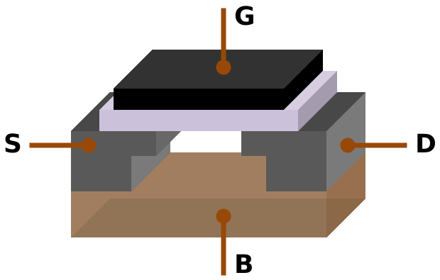
The gate, drain and source are different terminals. In an enhancement-mode N-channel MOSFET, making the gate sufficiently positive relative to the source increases channel conduction.
A threshold test at 250 µA checks just 0.00025 A. An illustrative 5 A load needs 20,000 times that current. Crossing the small-current checkpoint says little about the voltage drop at that load.
This ratio is a scale comparison, not a way to calculate the required gate voltage.
Read the whole threshold row: drain current, drain-voltage condition, temperature and notes. A common condition is VDS = VGS, with gate and drain tied for the measurement. It is not the normal wiring of a power switch. Conduction is continuous, and subthreshold current can exist below the listed threshold. See Nexperia's datasheet-parameter guide.
Which Gate-Voltage Specifications Must Be Kept Separate?
Keep VGS(th), the VGS condition for RDS(on) and the absolute maximum VGS rating separate. They describe the onset of conduction, a supported resistance test and a stress boundary—not three versions of one recommended drive voltage.
A specification such as “VGS(th) = 1–2 V” does not recommend driving the gate between 1 V and 2 V. It means devices reach the stated test current at different voltages within that range, under the listed conditions.
| Parameter | Question it answers | What it does not establish |
|---|---|---|
| VGS(th) | At what gate-source voltage is the small test current reached? | Low resistance at load current |
| VGS for RDS(on) | At what drive condition is this resistance limit specified? | Acceptable switching time or board temperature |
| Absolute maximum VGS | What gate-source stress boundary applies? | A recommended normal drive voltage |
The practical reading order: find a usable resistance specification, verify the available drive, then check gate stress in both polarities. Include overshoot and ringing, not only the settled DC voltage.
More gate drive can reduce resistance, but the benefit eventually becomes small. Moving toward the stress limit can increase oxide stress without a useful improvement. Follow the selected device's operating restrictions; Nexperia's gate-drive reliability note explains why voltage and temperature must be considered together.
“Fully on” is shorthand. The engineering target is adequately low, supported resistance at the required current and temperature—not merely a gate voltage above a threshold number.
What Do Real MOSFET Datasheets Show About Threshold and On-Resistance?
The cited IRFZ44NPbF and IRLML2502PbF specifications show that threshold voltage and guaranteed on-resistance belong to different test conditions. A buyer or engineer must preserve those conditions instead of transferring one headline value to another gate voltage.
Compare the conditions, not just the bold numbers. The IRFZ44NPbF datasheet and IRLML2502PbF datasheet provide a useful contrast. These are different device classes, not suggested substitutes.
| Item to read | IRFZ44NPbF | IRLML2502PbF |
|---|---|---|
| VDS rating / package | 55 V / TO-220 | 20 V / SOT-23 footprint |
| VGS(th) min–max | 2.0–4.0 V | 0.60–1.2 V |
| Threshold conditions | ID = 250 µA VDS = VGS | ID = 250 µA VDS = VGS |
| Maximum RDS(on) | 17.5 mΩ VGS = 10 V, ID = 25 A | 45 mΩ VGS = 4.5 V, ID = 4.2 A |
| Additional low-voltage resistance limit | No 2.5 V or 4.5 V limit in the cited table | 80 mΩ VGS = 2.5 V, ID = 3.6 A |
Source: electrical-characteristics tables, page 2 of each linked datasheet. Resistance measurements use short pulses to limit heating. The IRFZ44N note specifies pulse width ≤400 µs and duty cycle ≤2%. These test currents are not continuous-current guarantees on an arbitrary PCB.
What Does the IRFZ44NPbF Evidence Permit at 5 V?
For the IRFZ44N, the 17.5 mΩ limit belongs to 10 V gate drive. The fact that 5 V exceeds its threshold range does not establish that resistance at 5 V. A sample passing a light-load demonstration would not close this specification gap.
Decision: do not approve 5 V operation using that resistance value. Establish suitable drive or obtain device data supporting the intended operating point.
What Does the IRLML2502PbF Evidence Permit at 2.5 V?
The IRLML2502 has an explicit resistance limit at 2.5 V. That is relevant evidence for a circuit whose minimum delivered VGS stays above this level. Temperature, current and cooling still need assessment.
Decision: preserve the test conditions. Do not interpolate a new guaranteed 3.3 V resistance between the 2.5 V and 4.5 V rows. Its 20 V rating and small package also prevent treating it as an IRFZ44N replacement.
Can a 3.3 V or 5 V Signal Fully Drive This MOSFET?
Only if the minimum delivered gate-source voltage supports the required resistance and switching behavior. Start with the guaranteed controller or driver output under load, not its nominal supply label, then subtract relevant source-reference rise and other losses.
What Must a 3.3 V Controller Guarantee?
Look for a maximum RDS(on) limit at a gate voltage no higher than the minimum you can maintain. A 2.5 V or 1.8 V specification may be relevant. A typical curve showing some current at 3.3 V is not the same as a production resistance limit.
What If a 3.3 V Board Delivers Only 2.4 V of Gate Drive?
Assume a controller guarantees a 2.7 V high output under the relevant loading. Its MOSFET source can sit 0.3 V above the controller reference. The minimum available drive is:
VGS(min) = 2.7 V − 0.3 V = 2.4 V
A candidate with resistance specified at 2.5 V has a missing voltage margin. Its low threshold does not fix that. Improve the drive/reference arrangement or assess a device with a supported lower-voltage resistance specification.
What belongs in the review record: output-high limit and test load, source-rise allowance, applicable RDS(on) row, temperature assumption and remaining validation.
What Margin Does a 5 V Driver Need?
For another illustrative budget, a 4.6 V minimum driver supply minus 0.2 V of applicable output and reference losses gives 4.4 V at the device. That does not meet a 4.5 V resistance condition.
Use realistic loading. Gate charging is a transient demand; a gate-source resistor can add a DC load. Startup, undervoltage and shutdown behavior can differ from the normal settled high state.
Does the “Logic-Level” Label Prove GPIO Compatibility?
Toshiba's logic-level explanation refers to drive from 4–5 V logic and separately warns about output-current capability. The label alone therefore cannot establish compatibility with every 3.3 V GPIO. The numerical resistance and gate-charge conditions are more useful.
Where Should Gate-to-Source Voltage Be Measured?
Measure VGS between the MOSFET gate and source at the device, using a valid measurement method for the circuit voltage and switching speed. A gate-to-ground reading can overstate the real drive whenever the source rises above that reference.
The controlling voltage is VGS = VG − VS. Both voltages on the right must use the same reference. A current-sense resistor, wiring resistance or dynamic inductive voltage can lift the source above controller ground.
- Gate, relative to ground
- 3.3 V
- Source, relative to ground
- 0.4 V
VGS = 2.9 V
A 3.3 V gate-to-ground reading hides the source rise.
- Gate, relative to ground
- 17 V
- Source, relative to ground
- 12 V
VGS = 5 V
The gate must rise with the source to maintain the intended drive.
For a high-side N-channel switch, fixing the gate at a voltage above ground can leave too little VGS as the output rises. A floating or boosted driver can address this, but its supply method, startup sequence and duty-cycle restrictions must fit the application. TI's MOSFET design-mistakes guide discusses the high-side and low-side distinction.
How Should VGS Be Read for a P-Channel Device?
An enhancement-mode P-channel MOSFET generally turns on with its gate negative relative to its source. A source at 12 V and gate at 7 V produce VGS = −5 V. A negative threshold value is therefore not evidence of a fault. Check the signed specifications and both polarities of allowed gate stress.
Why Can a MOSFET Run Hot Even When VGS Exceeds Threshold?
The device may be inadequately enhanced, switching too slowly, carrying too much current or losing heat poorly. Threshold alone cannot distinguish these causes, so separate steady on-state loss from transition, diode, linear-mode and thermal-path losses.
How Do Temperature and On-Resistance Move?
For the silicon power MOSFETs discussed here, threshold generally falls as junction temperature rises, while resistance in the well-enhanced on state generally rises. A hot device can reach its threshold test current more easily yet dissipate more conduction power at the same load current. See Toshiba's gate-drive application note.
Check cold startup and minimum drive, then hot resistance and off-state margin. A typical temperature curve supports an estimate, not automatically a guaranteed worst-case value. Do not apply a universal temperature correction to every device.
How Is Conduction Loss Estimated?
Pconduction = IRMS2 × RDS(on)
For steady DC, RMS current equals DC current. For PWM, use the RMS current through this MOSFET over the full interval, not just average load current. With an ideal rectangular 5 A pulse at 50% duty, IRMS = 5√0.5 ≈ 3.54 A; using the 2.5 A average would understate conduction loss.
Assumed operating resistances for teaching only. These are not predictions for the named MOSFETs and are not calculated from VGS(th).
The cooling requirement can change substantially. If a separate temperature assessment raises 20 mΩ to 40 mΩ, the same 5 A causes 1 W. That is an assumed resistance change, not a universal thermal multiplier. Include switching and other losses before estimating junction temperature for the actual PCB and package.
Which MOSFET Operating Region Produces a Low-Loss On-State?
A low-loss MOSFET switch normally operates in the ohmic region while on. MOSFET saturation is different from the terminology used for a saturated bipolar-transistor switch.

In power electronics, linear-mode operation often means deliberately carrying current with significant drain-source voltage, as in current limiting. This can put the device in its saturation region. For an illustrative 5 A and 3 V across the device, loss is 15 W. Use VDS × ID and the appropriate safe operating area, not an unrelated low-resistance specification. Nexperia's linear-mode note explains the thermal-stability constraints.
What Must Be Checked During Fast Switching and Turn-Off?
Check gate charge, driver source and sink capability, transition waveforms, Miller coupling, dead time and the defined off state. Being above threshold does not establish a fast turn-on or immunity to unintended conduction.
The gate draws little steady leakage current, but charging and discharging it needs transient current. Read gate charge at relevant drain voltage, current and gate swing. A resistance-compatible MOSFET can still be a poor match for a weak driver at the required PWM frequency.
How Does the Miller Plateau Differ From Threshold Voltage?
- 1 / Gate charge buildsVGS rises and conduction develops. Crossing a small-current threshold is only an early checkpoint.
- 2 / Drain voltage changesThe gate waveform can flatten at the Miller plateau as gate-drain charge is supplied.
- 3 / Gate reaches its drive levelThe channel becomes more strongly enhanced as the remaining gate charge is delivered.
This is a conceptual turn-on sequence, not a measured waveform. The plateau level and duration depend on the operating conditions and drive path. Nexperia's gate-driver fundamentals separates these stages.
Why Can Low Average Gate Current Hide High Edge Current?
Assume 20 nC of gate charge and a 100 ns charging interval. Q/t gives 0.2 A average during that interval. At 20 kHz, Q × f gives just 0.4 mA average charging current from the drive supply.
Those numbers describe different time scales. The first is a rough charge-delivery estimate, not a full switching-time model or a guaranteed peak-current requirement. At a 5 V swing, QVf is about 2 mW of gate-drive energy consumption, before driver quiescent and other losses.
Gate resistance, driver output impedance and layout affect the transition. A larger resistor may reduce ringing but increase switching loss; a smaller one may increase edge speed and noise. There is no universal resistor value that makes every MOSFET safe.
Why Can an Off Command Still Allow a Gate Disturbance?
A fast change in drain voltage can couple current through gate-drain capacitance. If the gate circuit cannot remove it effectively, VGS can rise and cause unwanted conduction. In a half bridge, overlap can create a damaging current path. Infineon describes this dv/dt coupling mechanism.
A lower threshold can reduce disturbance margin, but threshold alone does not predict false turn-on. Driver sink impedance, capacitance, temperature and layout matter. Keep the gate-source loop compact and define the off state. A pull-down resistor helps with a floating control output; it does not automatically replace an effective driver during fast switching.
Which Bench Measurements Identify the Real Failure?
Capture VGS at the device together with VDS, current and relevant temperature evidence. Include startup, steady conduction, switching and turn-off; a multimeter average can miss a gate dip, overshoot, coupled disturbance or slow transition.
Probe safely. Use suitable differential/common-mode ratings, bandwidth and connection methods. Floating or high-side measurements may need a differential or isolated probe. Never defeat an oscilloscope's protective-earth connection. See the Tektronix probe primer.
| Observation | Possible issue | Useful next evidence |
|---|---|---|
| Hot with the switch steadily on | Low drive, high current or poor cooling | Actual VGS, on-state VDS, current and thermal conditions |
| Acceptable at DC, hot during PWM | Slow edges or other switching losses | Gate/drain/current waveforms at operating frequency |
| Starts warm, struggles cold | Insufficient margin or another startup problem | Minimum supply and cold-start sequence |
| Current spike during off command | Coupled gate disturbance, overlap or probe artifact | Source-referenced VGS and both-switch timing |
| Results vary between units | Tolerance sensitivity, assembly or part differences | Controlled conditions, part identity and comparison records |
Change one controlled condition at a time and keep the baseline traces. A lower case temperature after a change is useful evidence, but it does not establish acceptable junction temperature or voltage stress by itself.
What If a Replacement Passes a Lamp Test but Heats During PWM?
Suppose an alternative switches a steady load, yet runs hotter at the product's PWM frequency. Its threshold is similar to the original and its nominal resistance looks lower. That does not identify the cause.
Compare resistance at the actual gate drive, then compare gate-charge conditions and transition waveforms. Also review diode behavior, timing and cooling. The sensible next step is a controlled circuit comparison, not declaring the shipment defective from the threshold value or approving it from the DC demonstration.
What Evidence Is Required Before Selecting or Substituting a MOSFET?
Require the exact ordering code, circuit conditions, supported on-resistance, gate-voltage envelope, dynamic and thermal evidence, package and pinout before approval. Threshold similarity is not functional equivalence, and commercial availability does not replace electrical qualification.
- Describe the switching job
Record channel polarity, high-side or low-side position, load-current profile, supply range and transients.
- Build the gate-voltage envelope
State minimum and maximum VGS at the device, including startup, shutdown, source rise and ringing.
- Attach the applicable resistance evidence
Keep the maximum RDS(on) limit, test voltage, current, temperature and pulse conditions together. Identify typical-curve estimates separately.
- Check switching, thermal and protection limits
Review gate charge, driver capability, frequency, safe operating area, diode behavior and cooling. Confirm package and pinout rather than relying on a familiar outline.
- Control the commercial part identity
Send the full manufacturer part number and suffix, package, quantity, qualification requirements and allowed-alternative policy. Ask for the datasheet revision and an explicit list of differences.
A useful RFQ says what the circuit needs: “Please quote the exact part and flag any alternatives separately. On-resistance must be supported at our minimum gate-source drive; engineering validation of temperature and switching remains required.” Add your actual voltage, load and loss limits.
Review YURUNOX's purchasing process and quality-assurance information when defining the sourcing and documentation requirements. Incoming inspection and traceability support procurement control; they do not replace qualification in the intended circuit.
Send YURUNOX the exact part number, quantity, minimum gate-source drive, current profile, switching frequency and temperature requirements. Make the conditions part of the inquiry so proposed differences can be reviewed before an alternative is approved.
A datasheet comparison supports a decision. Circuit validation completes it.
Which Sources Should Be Rechecked Before Approval?
Reopen the current datasheet for the exact ordering code and retain every relevant test condition before design approval or purchase. The named devices illustrate how to read specifications; they are not a substitute list or a claim of stock availability. Numerical design and troubleshooting scenarios are explicitly illustrative, not YURUNOX test or customer results.
- Nexperia AN11158 Rev. 7.0 (18 February 2025): Understanding power MOSFET data sheet parametersThreshold conditions, subthreshold conduction, resistance and interpretation of ratings.
- Nexperia AN90001: Safe and reliable gate-drive operationGate-voltage limits, enhancement and reliability considerations.
- Infineon: IRFZ44NPbF datasheetPages 1–2: package, ratings and electrical-characteristics conditions.
- Infineon: IRLML2502PbF datasheetPages 1–2: low-voltage resistance limits and threshold conditions.
- Texas Instruments SLPA021 (November 2024): Avoid common MOSFET design mistakesGate-source drive, threshold and application-dependent selection.
- Toshiba AKX00068: MOSFET gate drive circuitDrive requirements, charge delivery and temperature trends.
- Nexperia AN50006: Power MOSFETs in linear modeOperating regions, dissipation, safe operating area and thermal stability.
- Nexperia AN90059: Power MOSFET gate driver fundamentalsGate charge, Miller plateau and driver considerations.
- Infineon: Effect of dv/dt on gate voltageDrain-to-gate coupling and unintended turn-on.
- Tektronix: ABCs of probes primerProbe ratings, source-referenced measurements and grounding safety.
Use the applicable current datasheet revision and manufacturer guidance for production decisions. Image credits and licenses appear beside each externally sourced visual.
Back to the top ↑