

Op-Amp vs Comparator: Why They Are Different
Use an op-amp to preserve or scale an analog signal. Use a comparator to report a threshold crossing. Similar symbols do not mean equivalent input limits, output interfaces or switching behavior.
Direct answer: Use an op-amp when negative feedback must produce a controlled analog value; use a comparator when the circuit must produce a threshold state. Do not approve a substitute from the symbol or package alone. Verify input limits, output architecture, recovery and timing, hysteresis, loading, exact ordering code and the evidence required by the application.
What Is the Practical Difference Between an Op-Amp and a Comparator?
An op-amp normally uses negative feedback to produce a controlled analog output. A comparator turns the relationship between two input voltages into a switching state. Choose the function first, then check the exact device. A spare amplifier channel is not automatically a suitable comparator.
For a sensor feeding an analog-to-digital converter, you may need amplification, buffering or filtering. For a sensor that must trigger an interrupt above a limit, you need a threshold decision. A product requiring both may need both functions, whether separate or explicitly integrated.
Scroll sideways to review the full decision gate →
| Circuit condition | Provisional choice | Evidence required | Stop boundary |
|---|---|---|---|
| The next stage needs a scaled, buffered or filtered analog value | Start with an op-amp in a valid feedback configuration | Gain, stability, input range, output swing, load and settling evidence | Stop if the required linear output cannot be guaranteed across operating conditions |
| The system needs a high/low event when a threshold is crossed | Start with a comparator | Trip accuracy, propagation delay, hysteresis and output-interface evidence | Stop if the receiving logic level, pull-up or timing remains undefined |
| A spare op-amp channel is proposed for threshold detection | Allow only after device-specific qualification | Input clamps, common-mode and differential limits, saturation recovery, supply current and startup tests | Do not approve when a critical behavior is unspecified or only a simulation passes |
| Procurement proposes a substitute with a similar package or pin count | Compare the complete ordering codes and circuit roles | Datasheets, pinout, package, grade, output type and application acceptance record | Reject a form-only match that changes the function or interface assumptions |
Scroll sideways to compare all columns →
| Decision factor | Op-amp | Comparator |
|---|---|---|
| Desired output | An analog value related to the input | A state indicating which input is higher |
| Usual feedback | Negative feedback sets the linear response | No linear feedback needed; positive feedback can add hysteresis |
| Speed to evaluate | Bandwidth, slew rate, settling and stability | Propagation delay and output transitions under stated conditions |
| Input difference | Normally kept small by a working linear loop | Often large in use, but still subject to device limits |
| Output interface | Analog load drive | Open collector/drain, push-pull or another specified interface |
| Typical job | Sensor scaling, filters, buffers | Threshold alarms, edge detection, voltage windows |
Analog Devices' Amplifiers as Comparators? explains why similar high-gain input stages do not make the finished devices interchangeable.
How Does Negative Feedback Change an Op-Amp’s Job?
Negative feedback makes an op-amp adjust its output toward a controlled analog relationship; a comparator normally operates as a switching decision element instead. The familiar triangle symbol does not make those operating goals interchangeable.
An op-amp responds to the difference between its plus and minus inputs. In a stable negative-feedback circuit, part of the output is returned in a direction that reduces that difference. The output settles to the value required by the feedback network, provided the input and output remain within their usable ranges.

Ideal noninverting gain = 1 + R2 / R1
R2 = 100 kΩ and R1 = 10 kΩ give a gain of 11 V/V.
For example, an ideal 100 mV input would become 1.1 V at that gain. This calculation neglects offset, finite gain and loading; it is not permission to demand an output beyond the available swing. Stability also depends on noise gain and load, not just the presence of a feedback resistor. ADI distinguishes noise gain from signal gain.
What Does a Comparator Do When Its Inputs Differ?
For the usual noninverting output convention, the comparator indicates high when the plus input is sufficiently above the minus input and low for the opposite relationship. An open output indicates high by releasing the node, not by actively driving it. Check the device truth table and any enable or latch controls.
The familiar op-amp approximation V+ ≈ V− applies to valid linear negative-feedback operation. It is not an internal short and does not apply to an open-loop comparator. Equal inputs also do not guarantee a stable comparator state: offset, noise and hysteresis influence the actual decision.
Which Input Limits Must Be Checked Before Making a Substitution?
Check common-mode operating range, differential-input behavior and absolute maximum stress as separate limits. Passing one does not establish valid operation under the other two.
A signal can be inside the supply rails and still be outside the specified operating range. Conversely, some devices explicitly support input conditions beyond a rail. Neither behavior should be inferred from a similar part number or a generic "rail-to-rail" label.
Scroll sideways to read all three checks →
| Check | Question to answer | Common mistake |
|---|---|---|
| Common-mode operating range | Are both input conditions valid for the specified behavior? | Assuming any voltage between the rails works |
| Differential-input limits | How far apart may the inputs remain, and what current can flow? | Ignoring clamps between the inputs |
| Absolute maximum ratings | Are voltage, current and other stress limits respected? | Treating a survival limit as a performance guarantee |
Some op-amps contain differential-input protection. When a comparison holds the inputs far apart, those structures can conduct and disturb the sensor or reference. A series resistor may limit stress without fixing switching behavior. TI's Bruce Trump describes this exact trap in Op Amps Used as Comparators—Is It Okay?
Check power sequencing too. A sensor may remain powered while the amplifier is off, or a reference may start first. Also investigate phase reversal where relevant: some devices can produce the wrong output polarity outside their valid input range. A "no phase reversal" statement does not waive the remaining limits.
What Output Interface Must the Next Circuit Receive?
Identify whether the next stage expects an analog voltage, an open-collector/open-drain node or an actively driven logic level. A correct threshold decision is still unusable when the output architecture conflicts with the receiving circuit.

Open collector and open drain describe outputs that can pull the node low but need a pull-up or another suitable load to establish high. "High" means the output transistor is off.
In an LM393-family circuit, an absent pull-up can leave the receiving input without a defined high level. Check the interface before assuming the IC is defective. TI's LM393-family datasheet explains the output and its dependence on resistance and capacitance.
How Does a Pull-Up Affect Rise Time and Sink Current?
A larger pull-up resistor reduces low-state current but charges the output capacitance more slowly. A smaller resistor speeds the rise while increasing sink-current demand and potentially raising the low-state voltage. Include the PCB, receiving pin and measurement probe in the capacitance estimate.
Illustrative RC calculation: 4.7 kΩ × 20 pF = 94 ns. For an ideal first-order node, the 10%–90% rise time is about 2.2RC, or 207 ns. This is the external rise after release, not the comparator's internal propagation delay.
What Must an MCU Check for a Push-Pull Output?
A push-pull comparator actively drives both high and low. It avoids a pull-up-controlled rising edge, but output levels and transition times still depend on load. Do not tie ordinary push-pull outputs together.
For an MCU connection, compare guaranteed output-high and output-low voltages at the required current with the MCU's input thresholds. Also check maximum pin voltage and power-off behavior. A 5 V push-pull output is not automatically safe for a 3.3 V input. An open output can sometimes support another pull-up voltage, but only within its documented ratings and sequencing conditions.
Which Speed Specification Matches the Real Event?
Use op-amp bandwidth, slew rate and settling only for their stated linear conditions; use comparator propagation delay with its supply, overdrive, load and transition direction. If an op-amp is driven into saturation, recovery must be qualified separately.
Bandwidth describes linear frequency response. Slew rate describes a large-signal output slope. Settling time describes reaching a specified accuracy. None alone establishes how quickly an op-amp will respond after being held at an output limit.
With negative feedback removed, internal amplifier stages may overload. After the input reverses, those stages can need time to recover before the output moves. ADI's MT-084 tutorial identifies this as a major uncertainty in comparator-style op-amp use.
What If the Input Is Slow but the Alarm Must Be Fast?
Imagine a temperature signal that changes gradually. The threshold circuit spends minutes in one output state, but the system requires a prompt interrupt once the limit is crossed. The low input frequency does not remove the recovery requirement. Test a long dwell followed by the smallest relevant threshold crossing, not only a repetitive square wave.
A comparator's propagation delay is measured between defined input and output events. Read the supply, load, overdrive and direction alongside the number. Input overdrive means the amount beyond the comparison level in the test setup—not permission to exceed an input rating.
For example, the TLV320x datasheet, section 6.6 lists typical low-to-high and high-to-low delays of 47 ns and 45 ns at 5 V, 20 mV overdrive and 15 pF load. These are conditional typical values, not universal maximums for every waveform.
The full alarm delay can also include input filtering, external output charging and MCU sampling or synchronization. An upstream op-amp that clips or recovers slowly can limit the response even if the comparator itself is fast.
Can an Op-Amp’s Supply Current Change When It Saturates?
Yes, for some devices and conditions. A linear-operation supply-current limit may not describe an op-amp held at an output extreme, so power and startup checks need device-specific evidence.
In a 2011 Analog Devices article, applications engineer Harry Holt measured devices as followers and with their outputs forced low or high. For the OP184 entry at 30 V, the reported supply currents were:
Scroll sideways to compare test states →
| Follower | Output forced low | Output forced high |
|---|---|---|
| 1.239 mA | 1.188 mA | 6.683 mA |
The forced-high measurement was about 5.4 times the follower measurement. This does not mean all op-amps behave that way; the article reports substantial variation between devices.
Decision consequence: when qualifying an amplifier for comparison, measure supply current in both held output states and during startup. A linear-operation current specification may not cover the proposed use. Source: The Maximum Supply Current That Wasn't, Table 1 and test descriptions.
How Does Hysteresis Set Rising and Falling Thresholds?
Positive feedback moves the comparison threshold after the output changes, creating one threshold for a rising input and another for a falling input. The separation reduces repeated switching near a noisy boundary but also changes the trip and release points.
A slowly moving signal can cross one threshold repeatedly as noise pushes it back and forth. Positive feedback adds hysteresis: after switching, the signal must reach a different threshold before the output reverses. TI's inverting-comparator hysteresis design note explains the principle.
Hysteresis is not extra measurement accuracy and does not remove input noise. It deliberately creates a switching band. Too much can postpone a required event or hold an alarm longer than intended.
Use Rref = 10 kΩ, Rfb = 330 kΩ and Vref = 1.65 V. If the output levels are ideally 0 V and 3.3 V, the plus-input node follows:
Vthreshold = (Rfb × Vref + Rref × Vout) / (Rref + Rfb)
The unrounded hysteresis width is about 97.06 mV. In a real design, include resistor tolerance, reference impedance, offset, input current, intrinsic hysteresis and output-voltage variation. An open-collector implementation also requires its pull-up and loading to be included in the network calculation.
What Should the Hysteresis Calculator Assume?
Change the resistor values or assumed output levels. These are nominal calculations for the schematic above, not component recommendations or a tolerance analysis.
Rising Vin: high → low
Falling Vin: low → high
Hysteresis width
The ideal model retains its previous state between the two thresholds. Displayed thresholds are rounded independently.
Scope: ideal push-pull output; no input current, offset, intrinsic hysteresis or resistor tolerance. This tool keeps Vref between the entered low and high levels. It does not check supply ratings, common-mode range, startup or switching speed.
Which Exact Device Examples Clarify the Difference?
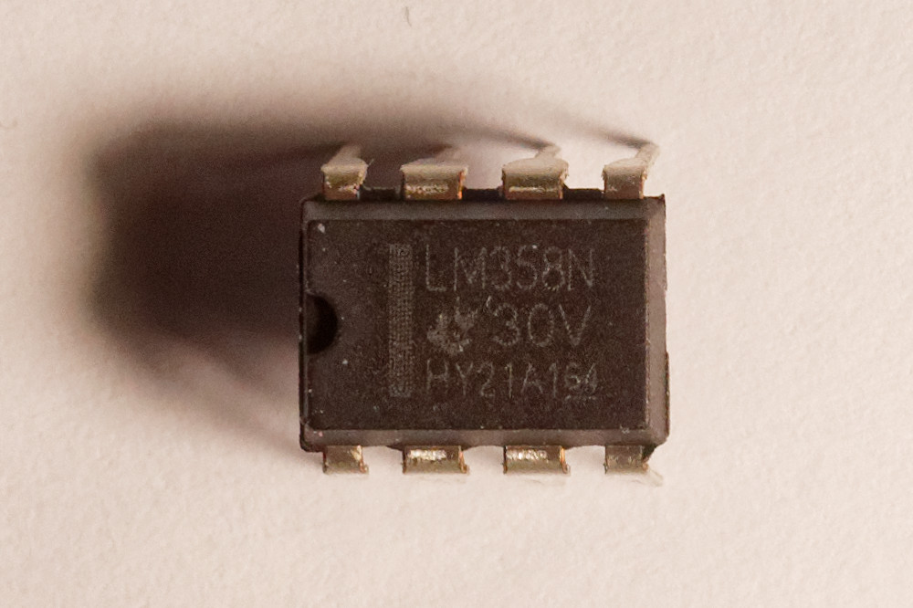
LM358B, LM393B and TLV3201 show three different roles: linear amplification, open-collector comparison and push-pull comparison. They are examples for reading the circuit requirements—not a substitution chain.
The suffix, package, channel count, pin assignment and electrical conditions all belong in the comparison.
Scroll sideways to compare device roles →
| Device | Published role | What to check first |
|---|---|---|
| LM358B | Dual operational amplifier | Gain accuracy, input range, output swing and linear stability |
| LM393B | Dual comparator; open-collector outputs | Pull-up network, sinking capability and input conditions |
| TLV3201 | Single comparator; push-pull output | Logic levels, load, overdrive and specified switching conditions |
An LM358B's amplifier specifications do not establish LM393B-equivalent behavior. Likewise, replacing an open-collector comparator with a push-pull type changes the circuit assumptions, especially if outputs are combined or pulled up to another rail.
For procurement, attach the actual ordering code and relevant datasheet revision. Use the Texas Instruments sourcing page as a starting point for an enquiry, not as evidence that a particular part is available or qualified for your circuit.
When Is an Op-Amp Acceptable as a Comparator?
Sometimes, if the manufacturer guidance and application evidence support that exact use. A slowly changing, noncritical indicator may tolerate behavior that a timed control or protection path cannot. If the required recovery limit is unspecified, one successful prototype does not create a production guarantee.
Simulation is useful for exploring the idea, but TI warns that macromodels may omit differential clamps or represent overload behavior poorly. Check the real device as well as the schematic. A circuit that switches in simulation can still load its reference or recover too slowly on the bench.
- Define the requirement. Record analog accuracy or trip thresholds, maximum response time and the receiving interface.
- Check all operating states. Include normal inputs, maximum differential voltage, slow ramps, startup and partial power-down.
- Test the loaded output. Observe both input pins and the output with the actual pull-up, capacitance and receiving circuit.
- Exercise recovery and noise. Hold each output state, then cross the threshold with the relevant small overdrive and input slope. Check chatter and supply current.
- Document the approved variant. Keep the ordering code, package, temperature grade, datasheet and acceptance conditions with the design record.
Which Measurement Should Follow Each Symptom?
Output never rises? Identify the output architecture and pull-up first. Repeated transitions near the threshold? Check the input, reference, hysteresis, supply decoupling and layout coupling. Delay after a long dwell? Separate amplifier recovery from external RC charging and MCU response.
For sourcing, provide function, supplies, input range, threshold accuracy, output type, timing, load, full part number, quantity and delivery needs. Have engineering approve substitutions against these conditions; align incoming documentation with your quality-assurance requirements.
Send the required op-amp or comparator ordering code together with supply voltage, input conditions, output type and quantity. If alternatives are acceptable, include the electrical limits they must meet.
Discuss op-amp or comparator sourcingFor safety-related functions, follow the applicable system design and validation process. This guide and its calculations are not a safety qualification.
Which Sources Should Be Rechecked Before Approval?
Reopen the exact current datasheet, application note and ordering-code documentation before design approval or purchase. Measurements below are attributed to their original publications. Gain, RC and hysteresis examples are illustrative calculations, not YURUNOX test results.
- Analog Devices: Amplifiers as Comparators? and MT-084 — architectural differences and crossover-use limitations.
- TI Precision Labs: Pros and Cons of Using an Op Amp as a Comparator and TI: Op Amps Used as Comparators—Is It Okay? — differential clamps, saturation recovery, output edges and simulation limitations.
- TI LM358-family datasheet (Rev. AB, revised October 2024), LM393-family datasheet (Rev. AH) and TLV320x datasheet (Rev. C, revised May 2024) — exact device roles and electrical conditions.
- ADI: The Maximum Supply Current That Wasn't — Harry Holt's historical supply-current measurements.
- TI SNOA997: Inverting Comparator With Hysteresis — positive feedback and threshold design.
Confirm current documentation for the exact ordering code before purchase or substitution. Photos illustrate component identity, not authenticity, stock availability or tested circuit performance.