

What Is GPIO? Input and Output Pins Explained
GPIO stands for general-purpose input/output. It is a configurable digital connection on a processor, microcontroller or I/O expander. An input reads a logic level; a push-pull output drives HIGH and LOW; an open-drain output pulls LOW or releases the line. Always verify the exact pin map, voltage limits, current capability and reset behavior before wiring.
A GPIO name describes a possible function, not a universal voltage, connector position or load rating. Software configuration cannot make an electrically incompatible button, LED, module, relay or industrial signal safe.
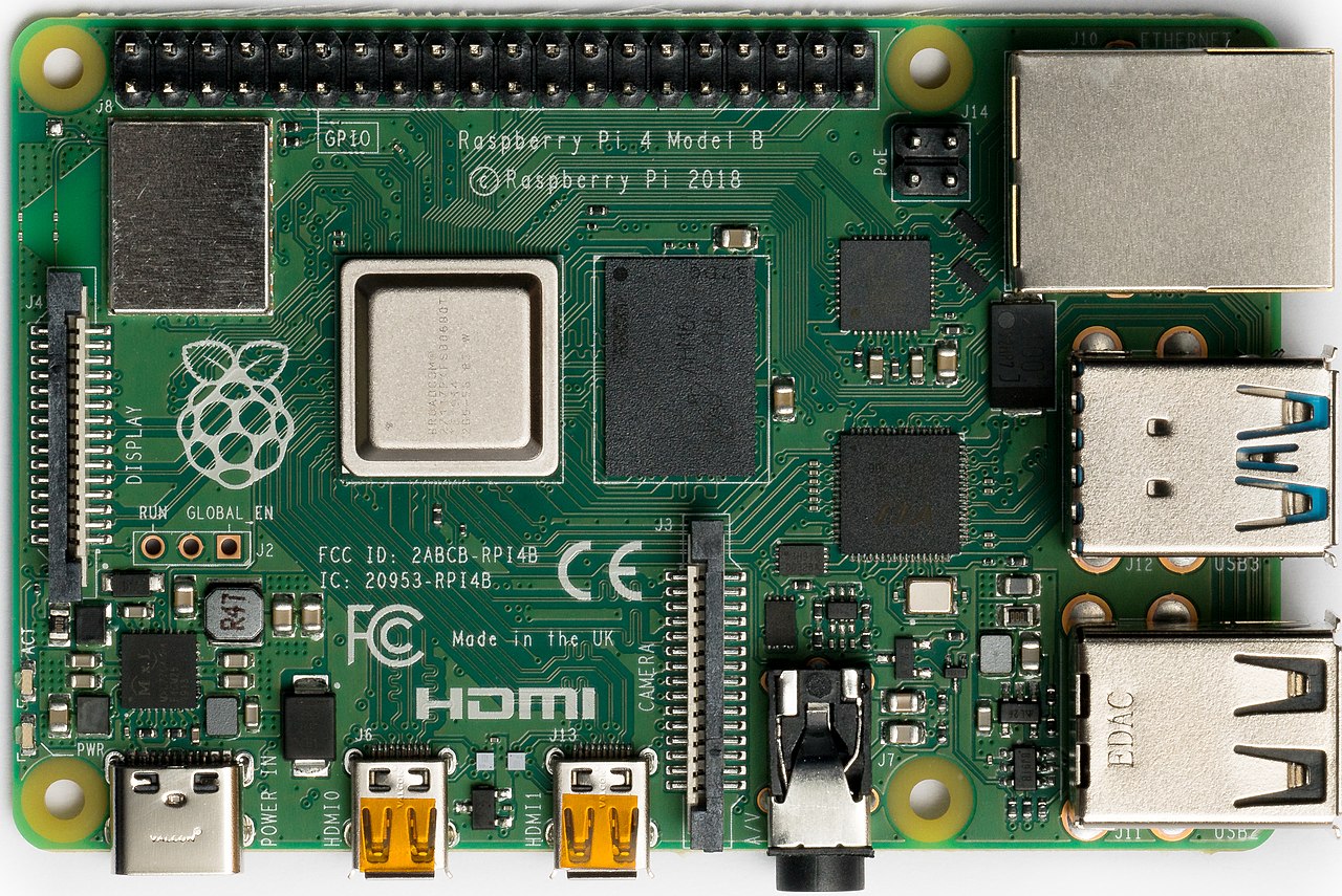 Raspberry Pi board with a GPIO header
What is GPIO, and how do input and output modes differ?
An input listens; an output controls. Direction is named from the processor's perspective. A sensor's output normally connects to the processor's input. A processor output may control a compatible enable input, indicator circuit or external driver.
Input: observes a voltage established by another circuit.
Output: drives the line within its electrical capabilities.
HIGH and LOW: logic states, not universal voltages.
Power and ground: different pin roles, even on a GPIO header.
Inside a typical GPIO block, an input buffer senses the pin and an output driver can control it. Configuration selects the available function, direction and bias. A microcontroller, processor or I/O expander may provide GPIO, but the details are device-specific.
| Condition | Recommendation | Evidence required | Stop boundary |
|---|---|---|---|
| Driven digital signal | Use a digital input with suitable bias only if the source can ever release the line. | Driver VOH/VOL, receiver VIH/VIL, voltage tolerance and shared reference. | Do not connect while either side's voltage domain or power-off behavior is unknown. |
| Button or open contact | Use an input with a permitted pull-up or pull-down and plan for debounce. | Switch wiring, internal/external pull, reset state, leakage and required event behavior. | Do not rely on an unconnected input as a stable HIGH or LOW. |
| Logic input or small LED load | Use push-pull only when the load and required state fit the pin's drive capability. | Loaded VOH/VOL, current, series resistance and combined bank/package limits. | Stop if the required current is based only on an absolute-maximum rating. |
| Shared or wired-AND line | Use open-drain with a calculated pull-up when every participant and the protocol support it. | Pull-up voltage, sink current, line capacitance, rise time and unpowered-pin tolerance. | Do not assume open-drain makes the pin 5 V tolerant. |
| Relay, motor, solenoid or 24 V signal | Use a suitable external driver, power supply and protection interface. | Load voltage/current, switching transients, isolation and fault requirements. | Never connect a raw GPIO directly to an incompatible power or industrial load. |
This is a triage guide, not a substitute for the exact device datasheet and board schematic. Scroll tables sideways on smaller screens.
Signal direction is not the same as current direction. An input can have leakage current, and an output can either source current into a load or sink current from it. For an ordinary non-isolated connection between boards, the signal also needs a suitable shared reference, usually ground. Do not bridge an intentional isolation barrier arbitrarily.
How do you identify the correct GPIO pin?
A board can have several naming systems at once: the processor's GPIO name, a development-board label and the physical position on a connector. The software library may use only one of them. A correct program targeting the wrong physical pin still gives the wrong result.
Where is GPIO17 on a Raspberry Pi header?
On the standard 40-pin Raspberry Pi computer header, GPIO17 is at physical pin 11. The same connector includes fixed power and ground connections. Raspberry Pi's computer documentation describes the GPIO signals as 3.3 V signals; the presence of 5 V supply pins does not make the GPIO inputs 5 V tolerant.
Write down both identifiers before wiring: signal GPIO17, connector position 11. Confirm connector orientation using the board pinout, and check which numbering scheme the software expects. This example concerns the standard Raspberry Pi computer header, not a Pico or an arbitrary carrier board. See the official Raspberry Pi GPIO reference.
The same discipline applies to production hardware. A signal named PA5 on a microcontroller is not automatically package pin 5. Package choice, board routing and alternate functions all affect the connection you can actually use.
How does a GPIO input recognize HIGH and LOW?
A digital input reports a logic state, not an exact voltage measurement. Its datasheet specifies guaranteed LOW and HIGH ranges. Between them, the interpreted state is not assured. Never assume the switching threshold is exactly half the supply voltage.
| Datasheet term | Meaning | Compatibility check |
|---|---|---|
| VIL(max) | Highest input voltage guaranteed to count as LOW. | Driver VOL(max) must not exceed this limit. |
| VIH(min) | Lowest input voltage guaranteed to count as HIGH. | Driver VOH(min) must meet or exceed this limit. |
| VOL(max) / VOH(min) | Guaranteed output levels at specified load and supply conditions. | Use the applicable current, temperature and supply conditions. |
| Permitted input voltage | Electrical operating limits, separate from logic recognition. | A recognized HIGH must also stay within the allowed range. |
Allow margin for noise and real operating conditions. A Schmitt-trigger input adds hysteresis: its rising and falling thresholds differ. That helps with certain slow or noisy signals, but does not remove voltage limits or solve every input problem. ST defines these terms in AN4899; use the exact device datasheet for numbers.
Why can an unconnected input change by itself?
A high-impedance input draws little current. Without adequate bias, leakage, interference or stored charge can move its voltage. This is a floating input, not a reliable default LOW. A reading that changes when you touch the wire is a reason to inspect the circuit.
Floating or excessively slow CMOS inputs can also increase supply current, as explained in TI's guidance on slow or floating inputs. A defined input state helps both reliable logic and power behavior.
When does a GPIO input need a pull-up or pull-down resistor?
A pull-up connects a signal through resistance to a permitted positive rail. A pull-down connects it through resistance to ground. Either can define the state when a switch or driver releases the line, without creating a direct supply short when the opposite state is applied.
Many controllers have internal pulls, but their availability, resistance and reset behavior vary. An external resistor can provide a more controlled bias or hold a state before firmware runs. Check for resistors already on the board before adding another.
An active-low button input
Assume a compatible 3.3 V input, a 10 kΩ pull-up and a normally open switch to ground. The values are teaching assumptions, not a universal circuit prescription.
Input reads HIGH
The open switch leaves the pull-up to establish the input voltage. The button is not active.
Ideal switch-path current: 0 mA. Real input leakage is not zero.
Pressed: the input connects to ground and reads LOW. Nominal pull-up current is 3.3 V ÷ 10,000 Ω = 0.33 mA. The demonstration omits contact bounce and parasitic effects; it is not a circuit test or simulation of a named board.
Active-low means the asserted condition is represented by LOW. If your button logic looks reversed, first compare the intended event with the wiring. Changing which state means “pressed” may be the correct fix; reversing power connections is not.
Lower pull resistance provides stronger bias but increases current when the line is LOW. Higher resistance reduces that current but may be less suitable with leakage, noise or capacitance. Choose the value from the complete interface rather than copying 10 kΩ automatically.
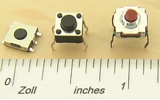 Tactile push-button switches
Why does a pull resistor not debounce the switch?
Contacts can bounce through several transitions during one press or release. A pull-up defines the open-switch level; it does not guarantee one event per press.
Use suitable firmware filtering or supported hardware debounce. An interrupt may capture unwanted bounce edges just as readily as a wanted edge. Microchip's GPIO debouncing lesson explains this distinction.
When should you use push-pull or open-drain output?
In output mode, software or a peripheral controls the output driver. The physical voltage still depends on the driver, load and external circuit. Writing HIGH to a register is not proof that the pin has reached a valid HIGH voltage.
- Push-pull output
- HIGH: actively drives toward the positive rail.
LOW: actively drives toward ground.
The output provides both drive directions. - Open-drain output
- Asserted LOW: conducts toward ground.
Released: stops driving the line.
A pull-up normally establishes HIGH.
Do not tie ordinary push-pull outputs together if they could drive opposing levels. One HIGH driver and one LOW driver can create contention and excessive current, including during startup or a fault.
For an open-drain line, the pull-up resistance and line capacitance affect the rising edge. A stronger pull-up charges the line faster but requires more sink current during LOW. TI demonstrates these behaviors using the TCAL6416 in its TCAL I/O-expander application note.
Ordinary bidirectional I²C uses compatible devices that pull shared lines LOW and release them for HIGH. It also has defined electrical and timing requirements; special modes have different rules. Use the NXP I²C specification, not the general-purpose label alone, to assess a bus.
Open-drain does not mean 5 V tolerant. When released, the pin is exposed to the pull-up voltage. Every connected device must permit that voltage in the relevant operating, reset and unpowered states.
Which GPIO voltage and current limits must you check?
Can a valid HIGH still exceed the pin's voltage limit?
A 5 V signal can exceed a 3.3 V receiver's HIGH threshold and still violate its permitted input range. Conversely, a 3.3 V output may not meet a particular 5 V receiver's HIGH requirement. Logic recognition and voltage tolerance are two separate checks.
Some devices offer tolerant pins, but the feature can depend on the specific pin, mode and supply state. ST's AN4899 distinguishes GPIO structures and cautions about analog functions and operating conditions. Do not extend one part's tolerance to every pin or every MCU in the family.
Use an appropriate level translator or interface circuit when voltage domains are incompatible. Its direction, output type, data rate and power-off behavior must match the application. A solution for one open-drain bus is not automatically suitable for a push-pull signal.
How much current can a GPIO output actually drive?
Check the current associated with guaranteed output-voltage levels, plus individual-pin and combined port, bank or package limits. A pin can stop meeting a valid logic level before reaching an absolute maximum rating. Absolute maximum current is a stress limit, not a normal design target.
Drive-strength settings are not precision current sources or protective current limiters. For a bare relay coil, motor or solenoid, use a suitable driver and power supply. Inductive loads also need a designed path for turn-off energy; TI discusses this in its inductive-load switching note. A relay module's control input is different from its coil, but still needs compatibility checks.
How do you size a resistor for a small LED?
For a sourcing arrangement, current flows from GPIO through a series resistor and LED to ground. Assume a loaded output of 3.3 V, an LED forward voltage of 2.0 V and a target current of 2 mA. These are illustrative values, not a rating for a named controller.
R ≈ (VOUT − VF) ÷ ILED
(3.3 − 2.0) ÷ 0.002 = 650 Ω
A 680 Ω resistor gives approximately 1.91 mA under the same assumptions.
Check the LED's forward-voltage range, resistor tolerance and power rating, and the GPIO's loaded output behavior. For a maximum-current estimate, use the highest credible drive voltage and lowest credible LED forward voltage. The arithmetic does not prove that every GPIO can supply 2 mA.
In a sinking arrangement, the LED circuit connects toward the supply and the GPIO draws current to ground. LOW may then turn the LED on. The circuit determines the active state; the words “input” and “output” do not.
Which analog, PWM and communication functions can a GPIO pin support?
A physical pin may connect internally to several blocks through a function selector, often called a multiplexer. Selecting analog input, a timer output or a serial peripheral changes which hardware uses the pin.
An analog-to-digital converter (ADC) returns a numeric representation of an input within its supported range. A digital GPIO read returns a logic state. Sharing the same physical pad does not make these operations equivalent.
Is PWM the same as an analog output?
Pulse-width modulation (PWM) switches an output repeatedly and varies its HIGH-time fraction, called the duty cycle. A 50% waveform spends half each cycle HIGH. It does not make the pin sit at half the supply voltage.
Which Arduino UNO R3 pins provide PWM?
Arduino lists pins 3, 5, 6, 9, 10 and 11 as supported PWM pins for the UNO R3. A spare digital pin is therefore not automatically interchangeable with a timer-connected PWM pin. The board's pin markings and official pinout help identify the available functions.
This is a concrete selection lesson: count the functions available in your actual pin assignment, not just the number of header positions. Other Arduino boards have different mappings. Source: Arduino's PWM pin guide. This is a public specification example, not a YURUNOX hardware test.
 Arduino UNO R3 digital and PWM pin labels
UART, SPI and I²C are serial communication functions, not alternative names for GPIO. If a peripheral owns a pin, changing an ordinary GPIO output value may not change the observed signal. Reserve required communication, analog, programming and debugging connections before assigning the remaining GPIO.
How do you configure and troubleshoot GPIO safely?
Use the exact device manual to implement this sequence. It is a planning workflow, not a universal register order.
- Identify the device and connection.Record the full part number, package, board revision, GPIO name and physical connector position.
- Review the complete circuit.Check existing pulls, loads, shared functions, supply domains and the reference connection.
- Configure the required function and electrical behavior.Select direction, bias, output type and supported edge-rate settings. Establish the intended inactive state using the documented initialization order.
- Check reset, startup, sleep and power-off.Where supported, preload the output latch before enabling the driver. Use suitable hardware bias if a load must stay inactive before firmware runs.
- Test one signal, then its real load.Measure at the physical pin and verify the input reading or output waveform. A successful software call does not prove correct wiring.
Should the input use polling or interrupts?
Polling reads the input periodically; an interrupt requests attention on a supported edge or level. A short pulse can fall between polls. An interrupt still needs correct setup, suitable handling and debounce where required.
For a button, define whether the application needs “pressed,” “released” or “held.” For precise pulse timing, consider timer capture or counting hardware. An ordinary software loop is not automatically a precise measurement instrument.
| Symptom | Possible cause | What to check |
|---|---|---|
| Input changes untouched | Floating input or interference. | Inspect bias and measure relative to the correct ground. |
| Button seems reversed | Active-low wiring. | Compare released and pressed voltages with the firmware interpretation. |
| One press, several events | Mechanical contact bounce. | Observe transitions and apply appropriate filtering. |
| Software changes; pin does not | Wrong mapping, disabled driver or peripheral ownership. | Check the physical pin, selected function and output enable. |
| Open-drain stays LOW | No pull-up, a short or another device pulling LOW. | Verify the pull-up rail and isolate possible pull-down sources. |
| Output sags under load | Excessive current or output contention. | Power down before rewiring; review the load and drive limits. |
If a controller appears powered while its main supply is off, investigate current entering through connected signals. Review power-off input behavior before continuing. For long cables or exposed connectors, provide the required interface and protection: a raw GPIO is not a rated 24 V industrial input. TI's GPIO ESD-protection guide explains why protection must match the interface.
What should an MCU or I/O-expander RFQ include?
Two devices with the same advertised pin count can have different usable functions, reset states, tolerances and drive limits. A proposed replacement needs a reviewed pin map and electrical comparison.
- Pin budget: required inputs and outputs after communication, analog and debug pins are reserved.
- Voltage domains: connected devices, supply ranges and required behavior when one side is unpowered.
- Output requirements: push-pull or open-drain, load current, pull resistors and external drivers.
- Timing and default states: interrupt, wake-up, PWM or capture needs; inactive states during boot, reset and sleep.
- Ordering details: full part number, package, temperature grade, quantity, delivery target and permitted alternatives.
Keep engineering compatibility separate from the evidence required for an offered component lot. YURUNOX's purchasing process and quality-assurance information provide useful next steps for a sourcing discussion.
Make your GPIO requirements clear before sourcing
Share the complete part number or BOM, pin-function needs, connected voltage domains and output loads. Add quantity, delivery target and approved alternatives so the sourcing discussion starts with the right component requirement.
Which sources support this GPIO guide?
Board examples use published documentation. Calculations and diagrams are illustrative; no physical circuit measurements or customer results are claimed. Always check the latest datasheet and schematic for the exact device and board revision.
- Raspberry Pi: GPIO and the 40-pin header — pin identity, supply pins and computer-GPIO signaling.
- STMicroelectronics AN4899, Rev. 4 — logic-level definitions, GPIO structures and operating-mode cautions.
- TI SCBA004: Slow or floating CMOS inputs — undefined inputs and power-consumption effects.
- Microchip: GPIO input handling and debouncing — switch bounce and event handling.
- TI SCPA070: TCAL Agile I/O expanders — programmable drive, pull resistors and output modes.
- NXP UM10204: I²C-bus specification — shared-line signaling and bus-specific requirements.
- TI SLVAF04: Inductive-load switching — external power stages and turn-off transients.
- Arduino: Use PWM output — board-specific PWM pin assignments.
- TI SLVAFQ4: ESD protection for GPIO — interface-specific protection considerations.
Photo sources and licenses appear with each image. For production, self-host optimized WebP copies in the WordPress media library and retain the adjacent attribution; external image URLs remain here as traceable source references. Product names identify technical examples and do not imply manufacturer affiliation or endorsement.