

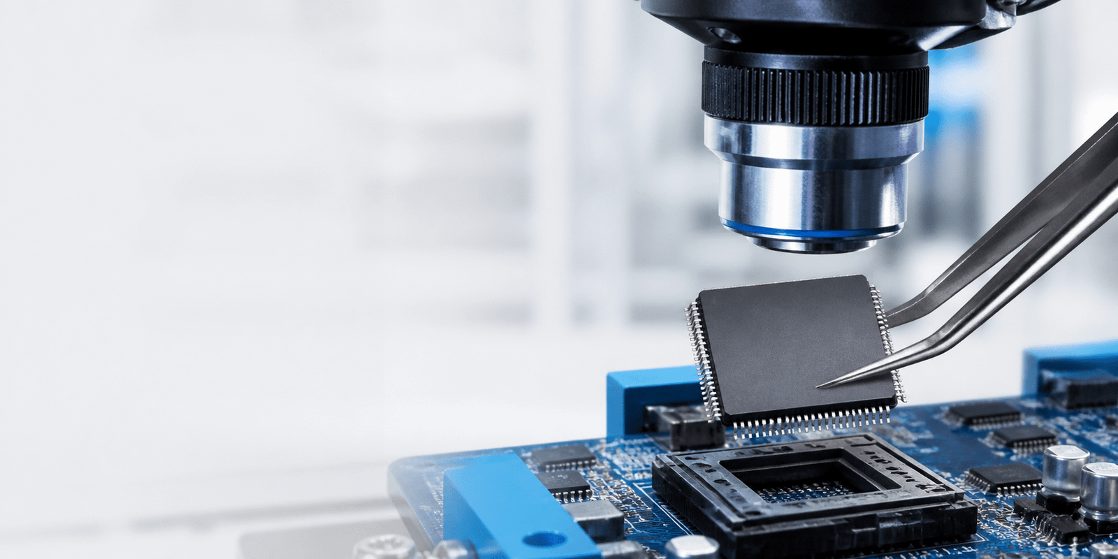
The complete material stack—from package to transistor
The word chip is used loosely. Sometimes it means the bare silicon die. In purchasing, it usually means a finished integrated circuit in a package. Those are different objects. A packaged processor, memory device, analog IC or power component combines several material systems that do different jobs.
At the bottom of the device hierarchy is a semiconductor wafer. Fabrication creates transistors and other structures on that wafer, then adds multiple insulating and conductive films above them. After wafer test and singulation, one or more dies are attached to a package structure, electrically connected, protected and tested again.

Substrate or leadframe, mold compound, lid, underfill and thermal interfaces
Protects · routes · coolsWire bonds, solder bumps, copper pillars or other package interconnects
Connects die to packageMany patterned conductor levels separated by low-k or other dielectric films
Moves signal and powerGate electrode, high-k dielectric, source/drain regions, contacts and isolation
Switches or sensesUsually single-crystal silicon; specialized devices may use SiC, GaN, GaAs or other materials
Forms the active foundationWhich materials appear in a chip, and what do they do?
There is no universal recipe. Foundries change materials as dimensions shrink, resistance rises or reliability requirements change. The table below is a practical map of commonly encountered roles—not a bill of materials for every device.
| Region | Typical materials | Primary job | Important caveat |
|---|---|---|---|
| Wafer and active region | Silicon; dopants such as boron, phosphorus or arsenic | Create controlled semiconductor behavior and transistor junctions | Silicon is a metalloid semiconductor, not the chip’s main wiring metal. |
| Gate stack | Hafnium-based high-k dielectric with metal-gate materials in many advanced processes | Control the transistor channel while limiting leakage | Hafnium here is part of a dielectric system; it is not an interconnect wire. |
| Contacts and vias | Tungsten, cobalt or other process-specific conductors | Carry current vertically between devices and wiring levels | The selected metal depends on geometry, resistance and integration scheme. |
| On-die interconnect | Copper or aluminum, with process-specific caps, liners and barriers | Route signals, clocks, power and ground across the die | Copper dominates many modern logic interconnects, but aluminum remains in some layers and technologies. |
| Barrier and liner | Tantalum, tantalum nitride, titanium-based films and emerging alternatives | Control diffusion, adhesion and interface resistance | These films are extremely thin and not present in the same way in every node. |
| Die-to-package connection | Gold, copper or silver wire; solder bumps; copper pillars | Connect die pads to package conductors | Gold is one option, not a universal ingredient in every modern package. |
| Package and thermal structure | Organic laminate, ceramic, copper alloys, epoxy mold compound, solder and thermal interface material | Protect the die, route signals to the board and remove heat | Construction differs significantly among QFN, BGA, CSP, leaded and advanced multi-die packages. |
Why silicon is the starting material even though it is not a metal
Silicon is useful because its electrical conductivity can be deliberately changed. Introducing controlled amounts of dopants creates regions with different carrier behavior; insulating films and gate structures then allow a transistor to switch current on and off. A good conductor alone cannot provide this controllable behavior in the same way.
Silicon also benefits from a mature manufacturing ecosystem and a stable native oxide. These advantages helped the industry build repeatable wafer processing, dense integrated circuits and large-scale manufacturing around silicon. The Semiconductor Industry Association describes semiconductor wafers as silicon or compound-semiconductor foundations that are processed with conductors, insulators and dopants to create electronic functions. [1]

What the wafer image does—and does not—tell you
The reflective disk identifies the substrate format. The functional device appears only after many repeated deposition, patterning, etching, doping and cleaning steps.
- A wafer can contain many individual dies.
- Metals are added later as contacts and interconnects.
- The finished component also needs package-level materials.
Electrical control
Doping, gates and junctions make current flow controllable. That switching behavior is the basis of digital logic and is also used in analog, sensing and power devices.
Manufacturing platform
Silicon is not used alone. Thin films are deposited, patterned, etched and modified repeatedly to build the device and its interconnect system layer by layer. [2]
Copper, aluminum and tungsten form the electrical routes
After the transistors are formed, they must be connected into working circuits. Fabrication adds patterned conductor levels separated by dielectric films. Local wiring connects nearby devices; higher layers distribute longer signals, clocks, power and ground. A complex chip can contain many wiring levels, but the number and material stack are process-specific.
Why copper became important
Aluminum was the long-standing integrated-circuit interconnect metal. Copper offers lower electrical resistance and strong electromigration performance when integrated correctly, but it can diffuse into surrounding materials. That is why copper interconnects rely on carefully engineered barriers, liners, deposition and planarization steps. IBM reported a manufacturable full-copper CMOS wiring technology in 1997, an important industry milestone. [3]
Aluminum and aluminum alloys served as the principal wiring material for generations of integrated circuits and remain useful in selected processes, upper layers and pads.
Damascene-style processes made it practical to form copper conductors inside patterned dielectric structures while controlling diffusion and surface planarity.
At very small dimensions, interface and size effects raise resistance. Engineers therefore optimize the whole conductor, barrier, liner, dielectric and via scheme—not just the bulk conductivity of one metal.
Research and advanced-node integration investigate alternative materials such as ruthenium for selected narrow interconnect features. Imec has demonstrated low-resistance ruthenium lines at very tight pitch, but that does not mean every production chip uses ruthenium. [4]
Why tungsten is still relevant
Tungsten has been widely used in contact and via structures because it can fill small features and tolerate semiconductor processing conditions. Its role is usually vertical or local rather than the long horizontal wiring often associated with copper. Newer schemes may replace or supplement it in certain structures to reduce resistance.
Gates, contacts, barriers and liners are not interchangeable
A material can be present in a chip without serving as a visible wire. Modern transistor and contact stacks contain extremely thin films chosen for work function, dielectric behavior, adhesion, diffusion control, interface quality and process compatibility.
High-k and metal gate
Hafnium-based high-k dielectrics can reduce leakage compared with simply making silicon dioxide thinner. A compatible metal-gate stack controls transistor operation. Intel documented its high-k and metal-gate implementation at the 45 nm generation. [5]
Barrier and liner films
Tantalum, tantalum nitride, titanium-based films and other materials may form barriers, liners or adhesion layers. Their job is to make the surrounding conductor system reliable, not necessarily to carry most of the current.
Local contact metals
Tungsten, cobalt and other process-specific materials can connect source, drain or gate regions to the first wiring level. The exact choice changes with node and device architecture.
Interface engineering
At nanometer dimensions, an interface may dominate resistance or reliability. Material selection is therefore a stack decision involving geometry, deposition, annealing and neighboring films.
Gold, copper, solder and epoxy are often package materials
A bare die is fragile and difficult to connect directly to a circuit board. Packaging protects it, fans microscopic connections out to practical board-level terminals and supports heat removal. Intel’s packaging overview describes die attach, substrate, epoxy encapsulation, lid or heat-spreader integration and testing as parts of turning a silicon die into a finished processor package. [6]
The electrical bridge between die and package is not always gold wire. Wire-bond packages may use gold, copper or silver alloy wire. Flip-chip constructions can use solder bumps or copper pillars. An Amkor flip-chip package example lists solder or copper-pillar interconnect and gold, silver or copper wire options within the wider package family. [7]

Fine wire links die pads to a leadframe or substrate
- Wire may be gold, copper or silver alloy.
- Leadframe or substrate routes the connection outward.
- Mold compound protects the die and wires.
- Common in many analog, power, memory and general-purpose packages.
Face-down bumps or pillars connect die to substrate
- Solder bumps or copper pillars create dense area connections.
- Underfill can reinforce the gap between die and substrate.
- Package substrate redistributes signals to board terminals.
- Useful where connection density, electrical path length or heat flow matters.
SiC, GaN and GaAs solve different device problems
Not every electronic function is best served by silicon. Compound and wide-bandgap semiconductors are selected when designers need properties such as higher electric-field strength, high-frequency performance, optical emission or efficient operation under demanding power conditions.

Material choice follows the operating problem
Wafer appearance is not a selection specification. Buyers still need the exact MPN, voltage and current ratings, switching behavior, package, qualification, lifecycle and approved alternatives.
- Use silicon for the broadest mainstream device ecosystem.
- Evaluate SiC or GaN when the power-system tradeoff supports it.
- Confirm package and qualification, not only semiconductor material.
Silicon carbide
SiC devices are used in high-voltage and high-power switching applications where efficiency, temperature capability and system power density can justify a different device platform.
Gallium nitride
GaN supports fast switching and high-frequency operation in selected power-conversion and radio-frequency applications. Device structure and substrate approach vary.
Gallium arsenide and related compounds
GaAs and other III-V materials are used where high-frequency or optical behavior is more important than compatibility with mainstream silicon logic.
The U.S. Department of Energy identifies SiC and GaN as wide-bandgap semiconductor materials that can enable smaller, faster and more efficient power-electronic components in relevant applications. [8] This is an application-level advantage, not a claim that either material replaces silicon across all chip categories.
Are rare-earth elements inside every chip?
No. “Rare earth,” “rare metal” and “critical mineral” are not interchangeable terms. Some chip technologies use elements that are geologically or strategically important, but many rare-earth uses are found elsewhere in an electronic system—magnets, phosphors, displays, optics or batteries—rather than in every semiconductor die. A product-level material declaration is more reliable than a generic list.
Why chip materials matter to availability and risk
Semiconductor production depends on highly controlled grades of silicon feedstock, metals, gases, photoresists, deposition precursors and packaging materials. A raw element may pass through purification, chemical conversion, deposition-target production and specialist fabrication before it reaches a wafer fab or assembly site. Disruption can therefore occur far beyond a visible chip factory.
The 2026 U.S. Geological Survey mineral summaries document the global production and supply context for many mineral commodities. [9] The Semiconductor Industry Association also describes polysilicon precursors, tungsten vias, copper interconnects and gallium-bearing compound semiconductors as examples of critical semiconductor material uses. [10]
Concentrated processing
Mining location is only one factor. Refining, high-purity conversion and semiconductor-grade qualification can be concentrated in a different region.
Long qualification cycles
A chemically similar substitute may still need extensive process and reliability qualification before a fab or package line can use it.
Hidden package variation
Two devices with similar electrical functions can use different die revisions, assembly sites, lead finishes or package-interconnect technologies.
Why a material list cannot authenticate a component
Knowing that a family may use copper interconnects or a gold-free package does not establish that an offered unit is genuine, unused or compliant with the requested specification. Authentication and release decisions need order-specific evidence: traceability where available, label and package consistency, date and lot information, visual review, documentation and any agreed testing scope.
What to confirm before buying a chip
If a material requirement comes from reliability, compliance, assembly or failure-analysis work, state that requirement explicitly. Do not assume that all devices in a family have identical die, lead finish or package construction across revisions and assembly locations.
Start with the orderable identity
The most useful sourcing request connects technical intent to a complete part identity and an acceptance plan. A generic phrase such as “copper chip” or “gold-bonded IC” is not enough.
- Complete MPN and manufacturer: include suffixes that define package, grade, packing or qualification.
- Application and electrical role: state whether the device is for compute, memory, RF, sensing, power or connectivity.
- Package and assembly constraints: specify package code, dimensions, lead finish, moisture handling and board-process limits.
- Quantity, target date and destination: make commercial and delivery assumptions visible.
- Date code, lot or country requirements: separate mandatory limits from preferences.
- Compliance and material evidence: request manufacturer declarations, RoHS/REACH information or package construction data when required and available.
- Inspection and test scope: agree which photos, label checks, visual inspection, X-ray, marking review or electrical tests are needed before release.
- Alternate authority: say whether alternates are prohibited, buyer-approved only or open to engineering review.
For independent-market or hard-to-find sourcing, keep the specification tied to the actual offered stock. Availability, condition, packaging, evidence and timing can change from one lot to another.