

ASIC vs FPGA: Key Differences and Which Fits Your Product?
Choose an FPGA when requirements are still changing, field updates matter, or you need hardware sooner. Consider a custom ASIC when the workload is stable and measured power, performance, integration, or lifetime-cost gains justify the larger upfront commitment.
First eliminate any route that cannot meet a non-negotiable technical requirement. Then compare verification risk, schedule, complete system cost and credible lifetime volume — not just clock speed or chip price.

Should You Choose an ASIC, FPGA, or Off-the-Shelf IC?
Evaluate an FPGA first when requirements are evolving, you need adaptable parallel interfaces, or the product must reach hardware validation before a custom chip could be fabricated.
Evaluate a custom ASIC when stable requirements make dedicated circuitry valuable enough to justify its development, manufacturing and revision commitments.
Neither route is automatically faster, lower-power or cheaper for every workload. An off-the-shelf dedicated IC may also solve the problem without either development effort.
Scope matters: this guide mainly compares commissioning a custom digital ASIC with implementing a design on a purchased FPGA. Buying an existing catalog ASIC does not mean funding a new custom-chip development program.
| Condition | Recommendation | Evidence required | Stop boundary |
|---|---|---|---|
| Requirements or interfaces are still evolving | Shortlist an FPGA | Resource use by type, timing margin, measured power, tool/IP access, update and lifecycle plan | Stop if the exact device cannot close timing, fit resources, meet power, or support a controlled update path |
| Workload is stable and repeat volume is credible | Commission an ASIC feasibility and business-case study | Frozen specification, process/package/test scope, NRE, recurring cost, schedule, qualification, and downside-volume model | Stop if the technical gain is unproven or the cash, schedule, revision, or lower-demand case cannot be carried |
| An MCU, processor, or catalog ASIC already meets the need | Buy and qualify the existing device first | Exact MPN and revision, datasheet limits, lifecycle status, supply route, qualification, and software burden | Stop custom development unless the existing solution fails a documented requirement |
| Field logic updates are mandatory | Use an FPGA or another controlled programmable subsystem | Configuration technology, authentication, recovery, reserved capacity, validation ownership, and supported update route | Stop if the chosen technology is one-time programmable or the update and recovery process cannot be qualified |
| Power, performance, or integration is a hard limit | Benchmark the FPGA route, then evaluate an ASIC if margin is inadequate | Same workload, precision, memory, I/O, duty cycle, PVT conditions, thermal boundary, and pass/fail target | Stop any route that fails the measured system requirement, regardless of its forecast unit cost |
How to use this table: eliminate options that fail a non-negotiable requirement first. Only then trade unit cost against flexibility and schedule. A low-price design that misses the power budget or launch date is not a feasible alternative.
What Actually Changes Inside an ASIC or FPGA?
An application-specific integrated circuit (ASIC) is designed for an application or application class. It can contain logic, memory, processors, interfaces and analog functions. Application-specific does not mean it can perform only one operation or cannot run software.
A field-programmable gate array (FPGA) supplies a manufactured set of resources that your design configures. A look-up table (LUT) implements a logic function; registers hold state. Programmable interconnect joins them into a circuit. Dedicated arithmetic, memory and interface blocks can perform work more efficiently than building everything from general-purpose logic. Altera's architecture overview describes this mix of logic, DSP and RAM resources.
ASIC: implement the circuit in silicon
The physical implementation is made for the design. Changing behavior later depends on the processors, registers or other programmability deliberately included in that hardware.
FPGA: configure an existing fabric
The tools fit the design into a particular device. Configuration data, often called a bitstream, sets the implemented logic and connections. It is not simply a CPU instruction program.
Simplified paths, not complete development flows. Both require verification and implementation checks. FPGA hard blocks and ASIC embedded processors blur a simple “fixed versus flexible” description, but do not erase the distinction.

Reprogrammable has practical limits
Microchip's FPGA introduction distinguishes volatile SRAM configuration from nonvolatile flash-based configuration. SRAM configuration must be restored after power loss; the system's boot arrangement determines how.
Antifuse devices are an important one-time-programmable exception. Do not promise field updates until you have checked the exact technology and update path.
Even a reconfigurable device cannot acquire extra pins, more memory capacity or unsupported physical interfaces through a new bitstream. Reserve resources for likely changes and plan validation, update authentication and recovery from an interrupted update.
SoC is not a third mutually exclusive category. A system-on-chip describes integration. A custom ASIC can be an SoC, while an SoC FPGA can combine a hard processor subsystem with programmable fabric. Compare the actual resources, not the label alone.
How Should You Compare ASIC and FPGA Performance and Power?
An ASIC gives the implementation team more freedom to optimize its datapath, memory and wiring. An FPGA must fit the selected fabric and routing. That is a reason to investigate ASIC optimization, not evidence for a universal speed multiplier.
Clock frequency is cycles per second. Throughput is completed work per second. Latency is the delay from an input to its output. Both ASICs and FPGAs can use parallel pipelines, and a pipeline can deliver results frequently while each individual result still takes several cycles.
200 MHz does not tell you the frame rate
A hypothetical image pipeline accepting one pixel per clock at 200 MHz has an ideal input capacity of 200 million pixels per second. If its interface supplies valid pixels only half the time, the accepted rate is at most 100 million pixels per second before other bottlenecks.
Decision consequence: benchmark memory traffic, interface stalls and complete-frame processing. A higher clock does not fix a starved pipeline.
Use the same input size, numeric precision, accuracy requirement and system boundary. Measure sustained throughput under realistic backpressure, the required latency statistic, and timing margin at relevant voltage and temperature conditions. A processor or GPU remains worth considering when existing hardware and software already satisfy the workload.
Power: keep the memory and board in the comparison
Tailored circuitry can reduce energy per task, but results depend on process technology, memory access, switching activity, frequency and duty cycle. Compare idle power, active power and energy per completed task separately. Include the relevant memory, interfaces and power-conversion losses.
AMD's UG907 power-estimation guidance emphasizes clock and input activity assumptions. A low estimate based on an unrealistic activity pattern is weak evidence. Check the model inputs, then validate representative operation on hardware when available.
For a battery product, model sleep and active periods. For an industrial enclosure, test sustained load at the intended ambient temperature. A device power estimate does not, by itself, establish acceptable junction temperature with the actual package, PCB and airflow.
How Do Development Time and Verification Risk Differ?
Purchased FPGA hardware can support interface tests, software integration and customer feedback without waiting for custom chip fabrication. It still needs a verified specification, timing closure, power review and product qualification. Reprogrammability is not permission to ship poorly tested logic.
For a custom ASIC, plan physical sign-off, manufacturing-test preparation, fabrication, packaging and silicon bring-up. Synopsys describes the ASIC development flow from architecture and RTL through implementation and tape-out. Tape-out is release of manufacturing design data, not delivery of qualified production parts.
Design for test (DFT) provides structures for manufacturing fault testing. It does not prove that the intended product behavior is correct. Both routes need functional tests for reset, stalled interfaces, clock-domain crossings and error recovery.
Ask which changes the product must survive
List likely changes explicitly: another sensor timing mode, a revised packet format, different numerical precision, added diagnostics or a security update. Decide which can be handled in firmware, which need programmable logic, and which would force a hardware revision.
Request a milestone plan tied to scope, reusable IP, acceptance criteria and manufacturing access. Avoid generic “FPGA in weeks, ASIC in months” promises. Include time and budget for hardware findings and requalification, not only the planned first pass.
When Does a Custom ASIC Become Cheaper Than an FPGA?
Non-recurring engineering (NRE) is the upfront development expense. A custom ASIC estimate may include design, verification, IP, tools, masks, test development and qualification. FPGA projects also have engineering, tools, IP and validation costs, even though the customer avoids a custom silicon tape-out.
Use equivalent scope. A bare ASIC die quote is not comparable to a complete FPGA board. Define recurring cost per completed system, including relevant package, test, companion components and assembly costs.
ASIC total = ASIC fixed cost + lifetime quantity × ASIC recurring cost
FPGA total = FPGA fixed cost + lifetime quantity × FPGA recurring cost
Usual crossover quantity = extra ASIC fixed cost ÷ recurring saving per system
The last equation describes the usual case where ASIC fixed cost is higher and recurring cost is lower. It is an arithmetic model, not an industry threshold. If there is no recurring saving, increasing volume does not repay the extra fixed cost.
Worked example: equal cost at 20,000 systems
Assume $80,000 fixed + $38 per system for FPGA, and $680,000 fixed + $8 per system for ASIC. The ASIC's extra $600,000 is recovered at $30 per system: $600,000 ÷ $30 = 20,000 systems.
All figures are illustrative planning inputs, not supplier quotations, market averages or typical costs for a process node.
| Lifetime quantity | FPGA total | ASIC total |
|---|---|---|
| 5,000 systems | $270,000 | $720,000 |
| 20,000 systems | $840,000 | $840,000 |
| 100,000 systems | $3,880,000 | $1,480,000 |
Read the forecast, not only the last row. At 5,000 systems, the cheaper ASIC recurring cost does not recover its extra commitment. At 100,000, the simplified model favors ASIC by $2.4 million. Neither outcome survives unchanged if the requirements, costs or demand change.
Test the Lifetime-Cost Assumptions
Replace the example values with like-for-like project estimates. This tool compares arithmetic cost only; it does not verify engineering feasibility or forecast reliability. Entries are not sent or stored by this tool.
- FPGA route total
- $840,000.00
- ASIC route total
- $840,000.00
Equal modeled cost at 20,000 systems.
Cost crossover: 20,000 systems. FPGA costs less below this point; ASIC costs less above it.
Assumes equal useful functionality and constant recurring costs across the modeled range. Add yield, test, redesign, inventory and support allowances only where not already included. Cash timing, lead time and engineering risk remain separate decisions.
Review conservative, expected and upside volume scenarios. A low lifetime-cost estimate can still demand unaffordable upfront cash or miss a launch. Conversely, a strict energy or integration constraint may justify an ASIC below the economic crossover if other feasible routes cannot meet it.
Where Do ASICs and FPGAs Make Sense in Real Systems?
Industry labels are not enough. Networking, machine vision, industrial control and machine learning can use either approach. The relevant questions are what must remain adaptable, what limits useful performance, and whether specialization pays for the complete system.
Catapult: FPGA hardware for a service workload
Microsoft's 2014 ISCA paper describes FPGA acceleration for Bing search on a deployment of 1,632 servers. The work considered performance, power and resilience in the surrounding service, not merely an isolated arithmetic kernel.
What to learn: FPGA hardware is not limited to disposable prototypes. It can serve operational workloads when its implementation and integration fit the requirement. This historical deployment is not a description of Microsoft's current fleet or a direct comparison against ASICs.
The first TPU: specialize around a defined task
Google's 2017 ISCA paper evaluates its first-generation Tensor Processing Unit, a custom ASIC deployed from 2015 for neural-network inference. Dedicated matrix computation and on-chip memory supported the targeted workload.
What to learn: a defined, valuable workload can justify specialized silicon. The paper compares that TPU with contemporary CPUs and GPUs, not FPGAs; its results must not be relabeled as an ASIC-versus-FPGA speed or power ratio.
Illustrative scenario: one vision platform, several camera variants
A machine builder expects several camera interfaces and image-processing variants. An FPGA is worth evaluating because the same hardware may support different validated configurations. First demonstrate the largest planned variant: I/O, memory bandwidth, timing, resources and sustained power must all fit.
If one pipeline later stabilizes and lifetime demand becomes credible, an ASIC feasibility study may make sense. That is a new decision using updated scope and cost estimates — not an automatic next step after the prototype. This is a hypothetical engineering scenario, not a reported YURUNOX customer project.
Do not turn “high volume” into a shortcut. High forecast volume cannot fix an unstable specification. Low volume does not rule out dedicated silicon when a hard technical constraint requires it.
Can an FPGA Design Become an ASIC?
Parts of the logical design can often be reused, but an FPGA bitstream is not an ASIC manufacturing file. Register-transfer-level (RTL) source describes logic and state transitions. The target-specific implementation must still be rebuilt and verified.
Synopsys describes shared-RTL prototyping flows for supported library components. That demonstrates conditional reuse, not universal portability of every FPGA primitive, licensed IP core or timing constraint.
- Remap the device-specific resourcesReview block RAM, DSP, clocking, transceivers and other hard blocks against the target libraries and interfaces.
- Check behavior and rightsConfirm IP production licenses, reset and initialization, memory behavior, clock-domain crossings and any latency change.
- Revalidate the physical implementationRecheck timing and power at the required process, voltage and temperature conditions. FPGA success is not ASIC sign-off.
- Plan the production transitionInclude DFT, package and PCB changes, manufacturing tests, silicon bring-up and product requalification.
Maintain a common functional specification and regression tests. If a new implementation changes pipeline latency or reset sequencing, make that change visible to software and system teams.
Structured ASICs are another route, not a guaranteed drop-in
Structured ASICs use a more predefined silicon platform with limited customization. The eASIC N5X product brief is one documented example of that approach. Evaluate platform fit, IP, package options, the supported conversion process and the current commercial offer separately.
Do not assume a migration preserves board compatibility or field programmability. A predefined platform still imposes limits, and its availability or cost benefit needs project-specific confirmation.
What Must Engineers and Buyers Verify Before Choosing an FPGA or ASIC Path?
Begin with the workload, required interfaces, sustained throughput, latency, power, startup behavior and environmental limits. Then document likely changes, expected lifetime quantity and support horizon. The ASIC or FPGA label alone establishes neither compliance nor supply continuity.
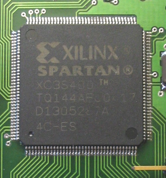
For an FPGA purchase
Specify the complete manufacturer part number, package, speed and temperature grades. Include configuration memory, power rails, clocks, companion memory and interface components in the BOM review.
Confirm lifecycle status, tool and IP requirements, traceability and the acceptable sourcing route. Compare resources by type, not only a headline logic count. Even the same package size does not establish pin or electrical compatibility.
Use Altera component sourcing or AMD component sourcing as a starting point for a specific enquiry, with the exact device requirements attached.
For a custom ASIC development commitment
Ask the design and manufacturing partners to define NRE scope, deliverables, acceptance milestones, process and IP assumptions, package and test scope, production pricing, minimum commitments and revision responsibility. Distinguish engineering samples from qualified production supply.
Clarify ownership and access to the design data, test program and support documentation. A custom design is not automatically portable to another foundry or process; an FPGA design is not automatically portable to another vendor.
Before approval, resolve these five questions
- Could an existing device solve it?Check suitable MCUs, processors or catalog application-specific ICs before funding a new hardware implementation.
- Is the critical path feasible?Demonstrate the demanding interface or datapath and record timing, memory, resource and power margins.
- What changes must remain possible?Identify the update mechanism, recovery process, reserved resources and validation owner.
- Does the business case survive lower demand?Compare complete costs and cash timing at several lifetime volumes, including an explicit revision contingency.
- Who owns long-term support?Name owners for configuration/software releases, test, product notices, supply interruptions and replacement qualification.
Match the sourcing route to the required evidence and inspection plan through YURUNOX Quality Assurance. Programmability is a technical capability, not a guarantee that a replacement part will be obtainable or interchangeable.
Which Technical Sources Support This ASIC and FPGA Comparison?
Manufacturer documentation supports the architecture and workflow explanations. Dated research illustrates applications; it is not a current product comparison. Cost and vision-platform examples are hypothetical, not supplier offers or first-hand customer results.
- Altera: FPGA Architecture OverviewProgrammable logic, routing, DSP and RAM resources.
- Synopsys: What Is ASIC Design?Custom hardware implementation and development flow.
- Microchip: What Is an FPGA? and FPGA Security GlossaryConfiguration technology and the antifuse exception.
- AMD UG907: Minimum Input Set2026.1 power-analysis guidance on clocks and representative activity.
- Microsoft Research: A Reconfigurable Fabric for Accelerating Large-Scale Datacenter ServicesISCA 2014; historical FPGA deployment for Bing search.
- Google Research: In-Datacenter Performance Analysis of a Tensor Processing UnitISCA 2017; first-generation inference ASIC. Not a direct FPGA comparison.
- Synopsys: FPGA Design Simplification with Synopsys IPShared-RTL prototyping with supported library components.
- eASIC N5X Product BriefStructured-ASIC platform example; availability and commercial suitability require confirmation.
Image credits and licenses appear below each photograph. Third-party names and images do not imply affiliation or endorsement.
Back to top ↑